Silicon negative electrode material with fluff structure and preparation method of silicon negative electrode material
A silicon anode and fluff technology, applied in structural parts, metal material coating process, battery electrodes, etc., can solve problems such as poor electrical conductivity and reduced electrical contact, to improve the pass rate, reliable electrical contact, and increase battery rate. performance effect
- Summary
- Abstract
- Description
- Claims
- Application Information
AI Technical Summary
Problems solved by technology
Method used
Image
Examples
Embodiment 1
[0038] SiO 2 Si powder, Si powder and 1wt% ferrocene were evenly mixed and placed in a chemical vapor deposition (CVD) furnace, heated to 1100 ° C, and the air pressure was kept at 500 Pa. After the deposition product was cooled, it was crushed and sieved to obtain iron-doped SiO powder, its diameter D50=5μm.
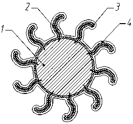
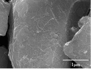
[0039] Heat the iron-doped SiO powder obtained in the previous step to 950°C in a CVD furnace. The vacuum in the furnace is controlled at 300Pa, and propylene with a flow rate of 9L / min and argon gas with a flow rate of 18L / min are introduced. The deposition time is 1h. Propylene was catalytically cracked to generate CNT fluff in situ on the surface of SiO powder, and the mass fraction of CNT fluff compared to the inner core was 3%.
[0040] Continue to heat the SiO / CNT composite powder obtained in the previous step to 950°C in a CVD furnace. The vacuum in the furnace is controlled at 300Pa, and propylene with a flow rate of 9L / min and argon gas with a flow rate of 18...
Embodiment 2-6
[0050] Other steps and process parameters are the same as in Example 1, the difference is that the physical properties of CNT are changed by controlling the deposition temperature, pressure and time; the thickness of the cladding layer of the fast ion conductor is changed by controlling the amount of fast ion conductor powder added. In addition, powder resistivity testing and secondary battery evaluation were performed in the same steps as in Example 1.
PUM
| Property | Measurement | Unit |
|---|---|---|
| thickness | aaaaa | aaaaa |
| thickness | aaaaa | aaaaa |
| thickness | aaaaa | aaaaa |
Abstract
Description
Claims
Application Information


