Broadband adjustable wave absorber with vanadium dioxide metamaterial loaded on dielectric layer

A vanadium dioxide and dielectric layer technology, applied in electrical components, magnetic/electric field shielding, antennas, etc., can solve the problems of narrow absorption spectrum bandwidth, single absorption peak, complex structure, etc., and achieve simple structure, improved bandwidth performance, and high The effect of absorption efficiency

Inactive Publication Date: 2020-08-11
TAIYUAN UNIV OF TECH
View PDF14 Cites 23 Cited by
  • Summary
  • Abstract
  • Description
  • Claims
  • Application Information

AI Technical Summary

Problems solved by technology

Although the adjustable absorber designed in the previous literature can realize the adjustment of the absorption frequency band, there are still shortcomings such as only a single absorption peak, narrow absorption spectrum bandwidth, and relatively complex structure.

Method used


Image

  • Broadband adjustable wave absorber with vanadium dioxide metamaterial loaded on dielectric layer
  • Broadband adjustable wave absorber with vanadium dioxide metamaterial loaded on dielectric layer
  • Broadband adjustable wave absorber with vanadium dioxide metamaterial loaded on dielectric layer

Examples


example 1

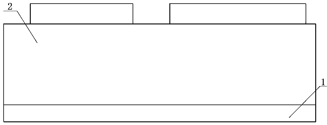
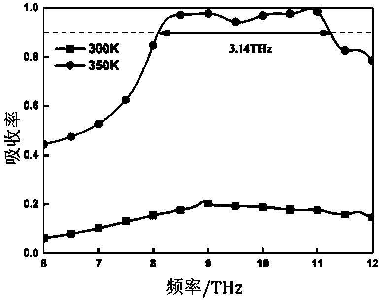
[0025] figure 1 , the cross-sectional side length P of the surface of the unit structure x =P y =50μm, the underlying metal film uses Au as the reflective layer, and the thickness of the metal film is h g =0.2μm; the dielectric layer adopts a dielectric constant of e r =4.3(1+0.025i) of FR-4 material, thickness h s=4μm; the resonant unit on the top layer consists of two groups of VO with different radii 2 The rings are arranged in the same plane, VO 2 The thickness of the ring is h r =0.2μm, the radius of the large ring is R=12μm, the radius of the small ring is r=8μm, and the radial width of the ring is w=3.5μm. Considering the convenience of actual processing, the cross-section of the ring structure in this embodiment adopts a rectangle, and other structures such as ellipse and circle are also acceptable. VO 2 The dielectric constant of the The high-frequency dielectric constant e in the formula ¥ =12, collision frequency g=5.75·10 13 rad / s, while the plasma freq...


PUM

PropertyMeasurementUnit
phase transition temperatureaaaaaaaaaa
thicknessaaaaaaaaaa
thicknessaaaaaaaaaa

Abstract

The invention belongs to the field of terahertz wave electromagnetic device design. The invention relates to a broadband adjustable wave absorber with a vanadium dioxide metamaterial loaded on a dielectric layer, which is characterized in that a metal layer, the dielectric layer and a vanadium dioxide VO2 resonant ring form basic units, and a plurality of basic units form a continuum array with aplanar array structure, so that the broadband adjustable wave absorber with the vanadium dioxide VO2 resonant ring loaded on the dielectric layer is formed. The structure is simple, experiment manufacturing is easy, the thickness is small, a new 'switching' function can be achieved on the wave absorber by adjusting the temperature, and more excellent wave absorbing performance such as bandwidth extension, polarization independence and incident angle insensitivity is achieved.

Description

technical field [0001] The invention belongs to the design field of terahertz wave electromagnetic devices, and in particular relates to the design of a novel broadband adjustable wave absorber formed by loading a metamaterial resonant structure based on a room temperature phase change material on a dielectric layer. Background technique [0002] Terahertz waves (THz) have the unique properties of high penetration and low photon energy, and will not cause damage to irradiated objects due to ionization effects, so they have great advantages in spectral analysis, imaging, radar and communication. At the same time, with the popularization and application of terahertz electromagnetic waves, its pollution problems also arise, so the study of terahertz wave absorption has become one of the very important topics. The absorber based on the absorbing mechanism is the most effective tool to eliminate electromagnetic pollution and realize electromagnetic protection. However, most mater...

Claims


Application Information

Patent Timeline
Patent Type & Authority Applications(China)
IPC IPC(8): H01Q17/00H05K9/00
CPCH01Q17/007H05K9/0081
Inventor 曹斌照李禹蓉任英楠费宏明刘欣张明达杨毅彪田媛
Owner TAIYUAN UNIV OF TECH
Why Eureka
Try Eureka