
Switch LDMOS device and manufacturing method thereof

A manufacturing method and device technology, which is applied in semiconductor/solid-state device manufacturing, semiconductor devices, electrical components, etc., can solve problems such as large device leakage on-resistance, device breakdown voltage drop, and large fluctuations in device characteristics. Low on-resistance, improved breakdown voltage, and good uniformity

Pending Publication Date: 2020-08-18
SHANGHAI HUAHONG GRACE SEMICON MFG CORP
View PDF4 Cites 0 Cited by
  • Summary
  • Abstract
  • Description
  • Claims
  • Application Information

AI Technical Summary

Problems solved by technology

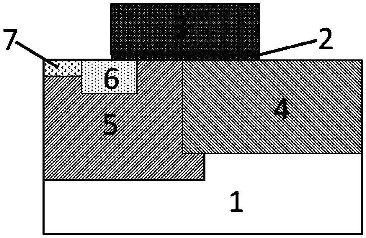
[0015] The technical problem to be solved by the present invention is to provide a switching LDMOS device and its manufacturing method, which can solve the non-self-alignment and short-channel effect between the non-self-aligned channel process, the drift region and the channel in the prior art The device characteristics fluctuate greatly, resulting in the decrease of device breakdown voltage, large device leakage and increase of on-resistance.

Method used


Image

  • Switch LDMOS device and manufacturing method thereof
  • Switch LDMOS device and manufacturing method thereof
  • Switch LDMOS device and manufacturing method thereof

Examples


Embodiment Construction

[0052] In order to illustrate the technical solution of the present invention more clearly, the accompanying drawings used in the present invention will be briefly introduced below. Obviously, the accompanying drawings in the following description are only some embodiments of the present invention. For those of ordinary skill in the art, In other words, other drawings can also be obtained from these drawings on the premise of not paying creative efforts.

[0053] The technical solutions in the present invention will be clearly and completely described below in conjunction with the accompanying drawings. Apparently, the described embodiments are part of the embodiments of the present invention, not all of them. Based on the embodiments of the present invention, all other embodiments obtained by persons of ordinary skill in the art without making creative efforts belong to the protection scope of the present invention.

[0054] Such as Figure 3 to Figure 8 Shown is a schematic...


PUM


Abstract

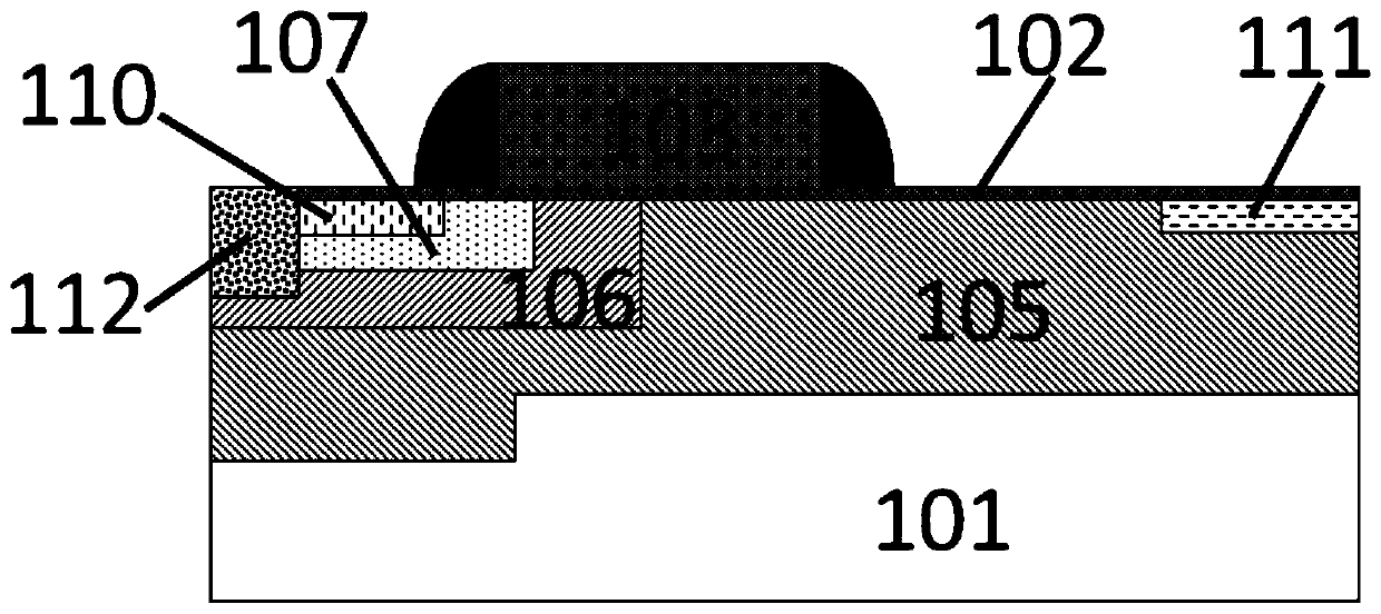
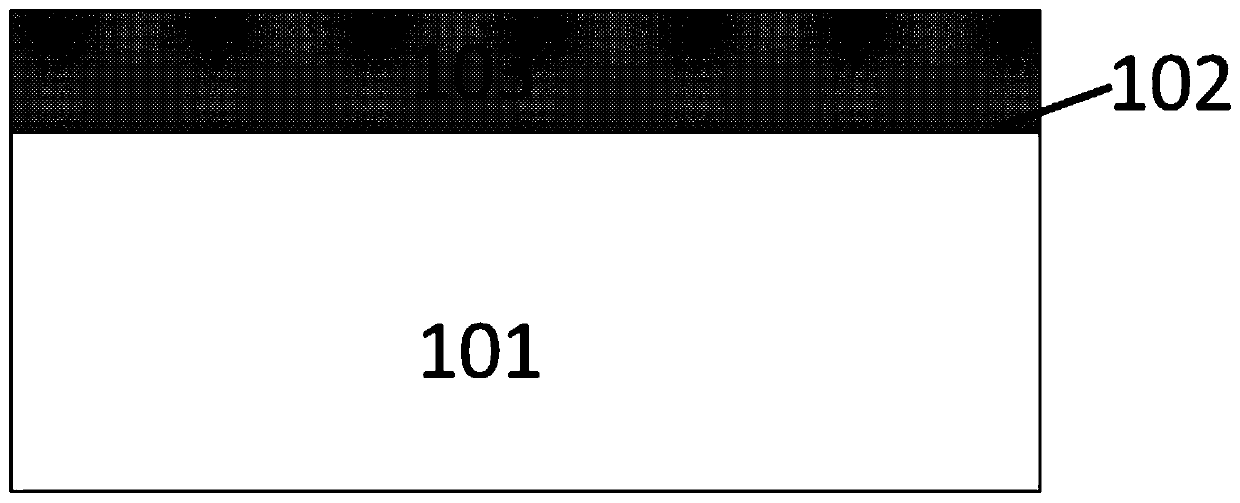
The invention discloses a switch LDMOS device, which comprises a drift region, a gate structure, a first conduction type channel region and a second conduction type source side lightly doped region, wherein the drift region is formed on a first conduction type semiconductor substrate and is distributed in all regions of the device; the gate structure is composed of a gate oxide layer and a polysilicon gate which are sequentially formed on the surface of the drift region; the first conduction type channel region is formed by angled ion implantation with the first side surface of the polysilicongate as a self-alignment condition and is completely located in the drift region, and the second conduction type source side lightly doped region is self-aligned with the first side surface of the polysilicon gate and is located in the channel region. The invention further discloses a manufacturing method of the LDMOS device. According to the invention, the polysilicon gate and the drift region are greatly overlapped, and the alignment of the polysilicon gate and the drift region does not influence the length of the channel; the length of the channel is determined by the angled ion implantation, and the short channel effect can be inhibited, so that the channel uniformity is better, the channel length can be reduced to the greatest extent to obtain ultralow on resistance, the breakdown voltage is kept or improved, and the electric leakage is kept or reduced.

Description

technical field [0001] The invention relates to the field of manufacturing semiconductor integrated circuits, in particular to a laterally diffused metal-oxide semiconductor (Laterally Diffused Metal-Oxide Semiconductor, LDMOS) device, and also relates to a manufacturing method of the LDMOS device. Background technique [0002] Low on-resistance is the main goal pursued by switching LDMOS devices, and lower on-resistance can greatly reduce switching power consumption. The on-resistance and breakdown voltage of LDMOS devices are a pair of mutually restrictive parameters. In the prior art, the methods for reducing the on-resistance while keeping the breakdown voltage constant include: [0003] 1) Through the RESURF (Reduced Surface Field) design, the electric field distribution in the LDMOS drift region can be made as uniform as possible, so that the doping concentration of the drift region can be appropriately increased; [0004] 2) Reduce the size of the device as much as p...

Claims


Application Information

Patent Timeline
IPC IPC(8): H01L21/336H01L21/265H01L29/78
CPCH01L29/66681H01L21/26513H01L21/26586H01L29/7816
Inventor 钱文生
Owner SHANGHAI HUAHONG GRACE SEMICON MFG CORP
Learn More