Photosensitization chemical-amplification type resist material, method for forming pattern, semiconductor device, mask for lithography, and template for nanoimprinting
A resist and light sensitization technology, which is applied in semiconductor/solid-state device manufacturing, photosensitive material processing, and photosensitive materials used in optomechanical equipment, etc., to achieve the effect of high sensitivity
- Summary
- Abstract
- Description
- Claims
- Application Information
AI Technical Summary
Problems solved by technology
Method used
Image

Examples
no. 1 Embodiment approach
[0040] The photo-sensitized chemically amplified resist material of this embodiment (hereinafter, simply referred to as "resist material" depending on the case) includes (1) basic components and (2) a photo-sensitizer and an acid that are generated by exposure. Element.
[0041] (1) Basic ingredients
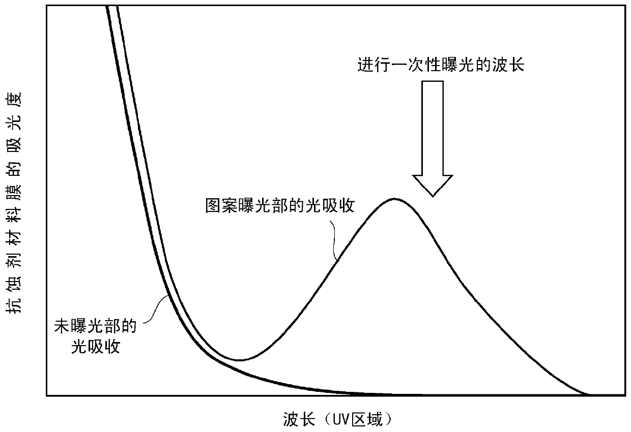
[0042] In this embodiment, the above-mentioned (1) basic component may be an organic compound or an inorganic compound. Also, the organic compound may be a high-molecular compound or a low-molecular compound. An ideal base component is a base component that does not excessively absorb the first radiation in the pattern exposure and can form a resist pattern having a shape with sufficiently high perpendicularity. In addition, among the base components, it is desirable that the absorption of the second radiation in the one-time exposure is small and the induction of unnecessary sensitization reaction in the unexposed part is less likely to occur during the one-shot exposure.
...
no. 2 Embodiment approach
[0208] The photo-sensitized chemically amplified resist material of this embodiment (hereinafter, simply referred to as "resist material" depending on the case) includes ( 1') Basic ingredients.
[0209] (1') Basic ingredients
[0210]The above-mentioned (1') basic component may be an organic compound or an inorganic compound. Also, the organic compound may be a high-molecular compound or a low-molecular compound. Among the three groups (d) acid-photosensitizer generating group, (e) precursor group, and (f) photoacid generating group, the above-mentioned (1') basic component has only the above-mentioned (d) ) or have any two of them, or have all of the groups represented by the following (d) to (f). That is, in the present embodiment, the above-mentioned basic component is an organic compound or an inorganic compound to which groups represented by the following (d) to (f) are bonded. The above-mentioned basic component may have groups represented by the following (d) to (f...
Embodiment 1
[0431] As methyl methacrylate to which a protective group is bonded, 32.19 parts by mass (0.44 parts by mole) of the following GBLMA, 23.86 parts by mass (0.24 parts by mole) of the following MAMA, and 21.29 parts by mass (0.21 parts by mole) of the following HAMA were mixed, and 22.66 parts by mass (0.11 parts by mole) of the following PBpS-F2MAS were mixed as methyl methacrylate to which a photoacid-generating group was bonded, and they were radically polymerized, thereby synthesizing a component having (f ) a photoacid generating group methyl methacrylate polymer compound (polymer compound P). The weight average molecular weight Mw of the obtained methyl methacrylate polymer compound was 24800, and the molecular weight distribution Mw / Mn was 3.08. In addition, the above-mentioned Mw and Mw / Mn are measured by gel permeation chromatography (GPC) under the following conditions using a calibration curve based on standard polystyrene.
[0432] Apparatus: HPLC (manufactured by S...
PUM
| Property | Measurement | Unit |
|---|---|---|
| wavelength | aaaaa | aaaaa |
| wavelength | aaaaa | aaaaa |
| wavelength | aaaaa | aaaaa |
Abstract
Description
Claims
Application Information
 - R&D
- Intellectual Property
- Life Sciences
- Materials
- Tech Scout
- Unparalleled Data Quality
- Higher Quality Content
- 60% Fewer Hallucinations
Browse by: Latest US Patents, China's latest patents, Technical Efficacy Thesaurus, Application Domain, Technology Topic, Popular Technical Reports.
© 2025 PatSnap. All rights reserved.Legal|Privacy policy|Modern Slavery Act Transparency Statement|Sitemap|About US| Contact US: help@patsnap.com