P-type MOSFET and manufacturing method thereof

A manufacturing method, N-type technology, applied in semiconductor/solid-state device manufacturing, electrical components, circuits, etc., can solve the problems of large influence on device threshold voltage, inability to improve hole mobility, large fluctuations in phosphorus ion implantation depth, etc. , to improve mobility and improve device performance

Pending Publication Date: 2020-08-25
SHANGHAI HUALI INTEGRATED CIRCUTE MFG CO LTD
View PDF6 Cites 1 Cited by
  • Summary
  • Abstract
  • Description
  • Claims
  • Application Information

AI Technical Summary

Problems solved by technology

In the prior art, the N well is usually implemented by implanting a layer of phosphorus ions, and the depth of phosphorus ion implantation fluctuates greatly, which greatly affects the threshold voltage of the device.
At the same time, in order to impr

Method used


Image

  • P-type MOSFET and manufacturing method thereof
  • P-type MOSFET and manufacturing method thereof
  • P-type MOSFET and manufacturing method thereof

Examples


Embodiment Construction

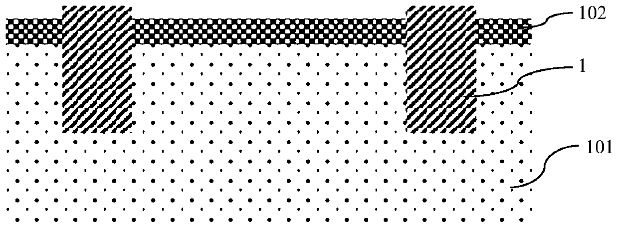
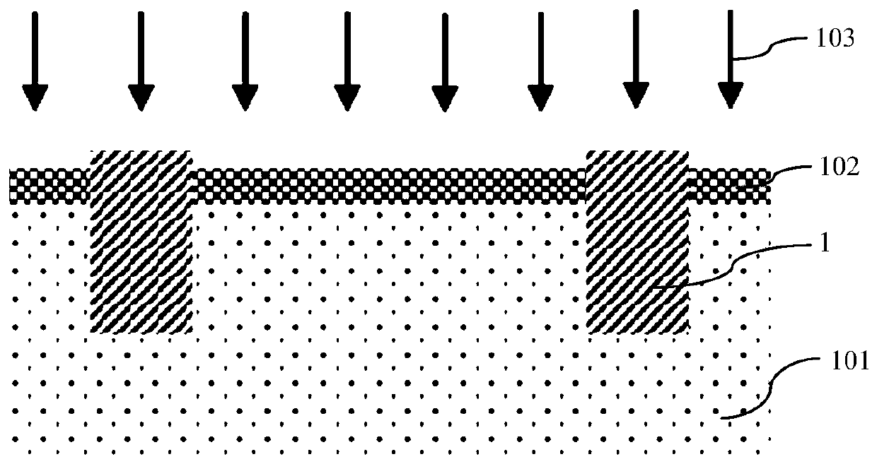
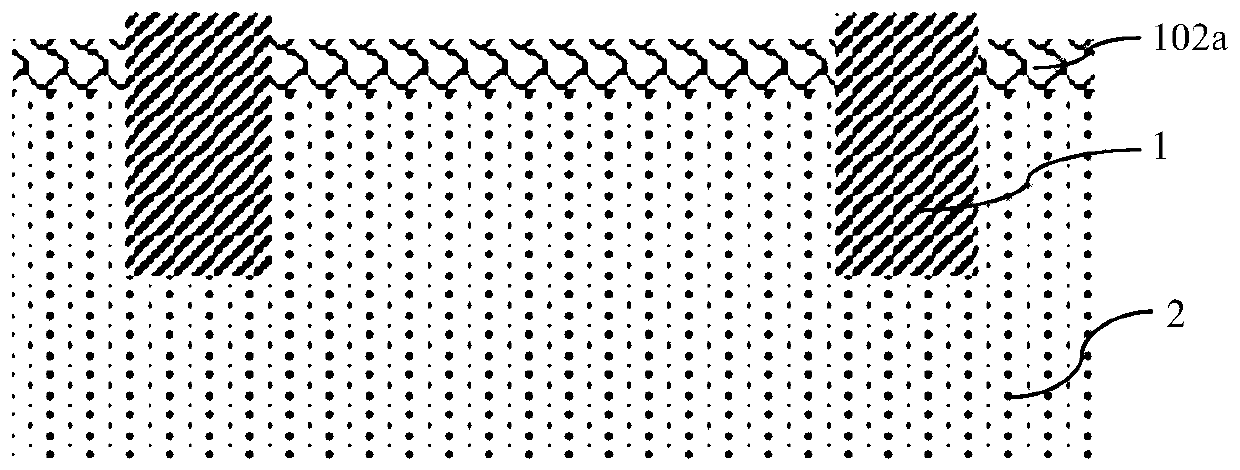
[0077] The structural reference of the channel region of the P-type MOSFET in the embodiment of the present invention Figure 1J and Figure 1K As shown, the channel region is composed of an N well 9 covered by a gate structure, and the N well 9 includes a first implantation region 4, a second implantation region 5, and a third implantation region 6 formed in a semiconductor substrate 101. The overlapping region 8 formed with the fourth implantation region 7 is annealed, that is, the N well 9 is formed after the overlapping region 8 is annealed. For the semiconductor substrate 101 please refer to Figure 1A as shown, Figure 1J Only the structure of the N-type deep well 2 formed in the semiconductor substrate 101 is illustrated in FIG.

[0078] In the embodiment of the present invention, the semiconductor substrate 101 includes a silicon substrate.

[0079] Preferably, a field oxide layer 1 is formed on the semiconductor substrate 101, and the active region is isolated by ...


PUM


Abstract

The invention discloses a P-type MOSFET. A channel region is composed of an N well covered by a gate structure, the N well comprises a superposition region composed of first to fourth injection regions, and the superposition region is subjected to annealing treatment; the injection impurities of the first to fourth injection regions are respectively phosphorus, germanium, xenon and arsenic, and the junction depths are sequentially reduced, wherein the doping concentration of the fourth injection region is used for adjusting the threshold voltage, the ion injection process of the fourth injection region is carried out after the ion injection process of the second injection region and the ion injection process of the third injection region are completed, and the second injection region and the third injection region form an amorphous layer in the semiconductor substrate to enable arsenic injection in the fourth injection region to be uniform, wherein the germanium impurities in the second injection region are used for providing pressure stress for the channel region; and the xenon impurities in the third injection region are used for preventing the germanium impurities from diffusinginto the fourth injection region so as to reduce defects caused by germanium diffusion. The invention further discloses a manufacturing method of the P-type MOSFET. According to the invention, the local fluctuation of the threshold voltage can be reduced, the channel carrier mobility can be improved, and the device performance and the product yield can be improved.

Description

technical field [0001] The invention relates to the field of semiconductor integrated circuit manufacturing, in particular to a P-type MOSFET. The invention also relates to a manufacturing method of the P-type MOSFET. Background technique [0002] The P-type MOSFET, that is, the PMOS, is usually formed in an N-type deep well (Deep Nwell layer, DNW), and the channel region is formed by using the N well. The ion implantation process of the N-type deep well is generally placed before the ion implantation process of the N well. The implantation energy of the ion implantation process of the N-type deep well is large, and the implantation depth is deep. Before the ion implantation of the N-type deep well, it is usually necessary to form a pad oxide layer on the surface of a semiconductor substrate such as a silicon substrate, and the ion implantation of the N-type deep well will pass through the pad oxide layer. [0003] However, after the ion implantation process of the N-type...

Claims


Application Information

Patent Timeline
IPC IPC(8): H01L29/78H01L29/06H01L29/10H01L29/36H01L29/167H01L21/336
CPCH01L29/78H01L29/7838H01L29/0607H01L29/0684H01L29/1054H01L29/36H01L29/167H01L29/66477
Inventor 李中华王海涛
Owner SHANGHAI HUALI INTEGRATED CIRCUTE MFG CO LTD
Why Eureka
Try Eureka