Manufacturing method of nano grating with high depth-to-width ratio

A nano-grating, high aspect ratio technology, applied in the coupling of optical waveguides, optics, light guides, etc., can solve the problem of slow electron beam direct writing speed, easy to cause defects, and low photoresist and nano-imprinting resist etching selection ratio. and other problems, to achieve the effect of good optical processing effect and easy preparation

Pending Publication Date: 2020-09-01
杭州欧光芯科技有限公司
View PDF10 Cites 5 Cited by
  • Summary
  • Abstract
  • Description
  • Claims
  • Application Information

AI Technical Summary

Problems solved by technology

In the above two technical solutions, due to the low etching selectivity ratio of photoresist and nano-imprint glue, it is impossible to fabricate a grating structure with a high aspect ratio or there are great difficulties in fabricating a grating structure with a high aspect ratio
In addition, ordinary lithography cannot process gratings with a period of nanometer scale. The speed of direct writing with electron beams is too slow, and lithography equipment such as stepping or EUV is too expensive and the cost is too high.
If only nanoimprinting is used to fabricate high aspect ratio grating structures, it is difficult to release the mold and easily cause defects

Method used


Image

  • Manufacturing method of nano grating with high depth-to-width ratio
  • Manufacturing method of nano grating with high depth-to-width ratio
  • Manufacturing method of nano grating with high depth-to-width ratio

Examples


Embodiment Construction

[0041] In order to further illustrate the technology and effects adopted by the present invention to achieve the intended purpose, the preferred embodiments of the present invention will be described in detail below with reference to the accompanying drawings.

[0042] In the following example, a preparation method of a grating with a line width of 150 nm and a height of 5 μm is described, including the following main steps:

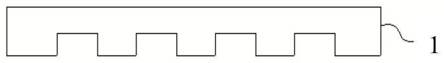
[0043] Step 1: A silicon wafer with a grating structure with a line width of 150nm and a height of 150nm is fabricated using traditional photolithography technology, as the original hard mold, which is a hard matrix nanoimprint mold.

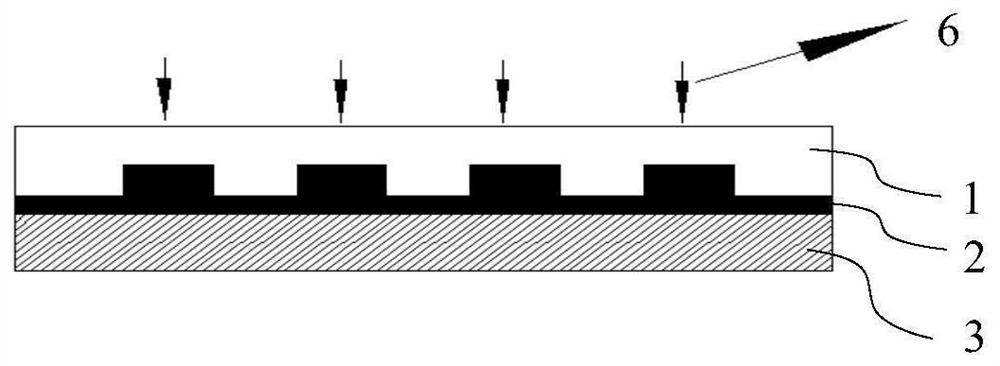
[0044] Step two, nanoimprinting, such as Figure 1a - Figure 1d Shown:

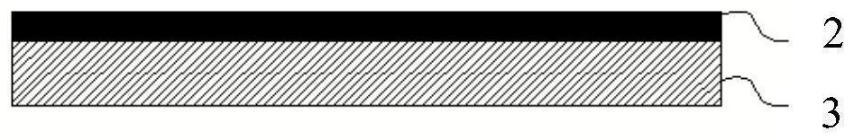
[0045] (1) Preparation of soft mold, spin-coat the hard mold prepared by step 1 at a speed of 3000r / min to obtain a layer of 4.5um polydimethylsiloxane adhesive layer, and polydimethylsiloxane adhesive layer is obtained by hot embossing process Me...


PUM

PropertyMeasurementUnit
widthaaaaaaaaaa
quality scoreaaaaaaaaaa

Abstract

The invention discloses a manufacturing method of a nano grating with a high depth-to-width ratio. The method comprises: manufacturing an original mold: manufacturing the original mold with a gratingstructure with a low depth-to-width ratio; carrying out nanoimprint lithography, and copying the grating structure through a nanoimprint lithography process to prepare a PDMS soft template; spin-coating nanoimprint lithography glue on a glass substrate to form a pattern transfer layer, covering the pattern transfer layer with a PDMS soft template, and separating and demolding after curing; removing the imprinting adhesive residual layer; plating a layer of metal on the glass substrate to form a metal layer; soaking and stripping the whole glass substrate from the falling pattern transfer layerand the metal layer on the falling pattern transfer layer to form a metal nanostructure mask; and etching the surface to form a nano grating structure with a high depth-to-width ratio on the surfaceof the glass substrate. According to the invention, the nano grating substrate with high depth-to-width ratio can be obtained by further processing on the basis of the nano grating substrate with lowdepth-to-width ratio, and the nano-scale grating structure with high depth-to-width ratio is obtained.

Description

technical field [0001] The invention relates to a method for manufacturing a nano-grating in the technical field of manufacturing micro-nano devices, in particular to a method for manufacturing a nano-grating with a high aspect ratio. Background technique [0002] Nanoimprint technology, first proposed by Professor Stephen Y Chou in 1995, is an important technology in the fabrication process of micro-nano devices. It is a new pattern transfer technology different from traditional lithography technology. Nanoimprint technology does not Use light or radiation to photosensitively shape the photoresist, which is to press the pre-prepared mold into the liquid resist, so that the resist will be physically deformed to achieve patterning of the resist, rather than by changing the resist The chemical properties of the corrosion resist are realized. Compared with traditional photolithography technology, it has the advantages of higher yield, lower cost and simpler process. [0003] ...

Claims


Application Information

Patent Timeline
Patent Type & Authority Applications(China)
IPC IPC(8): B81B7/00B81B7/04B81C1/00
CPCB81B7/00B81B7/04B81C1/00015B81C1/0046B81C1/00349
Inventor 张琬皎龙眈张颖
Owner 杭州欧光芯科技有限公司
Why Eureka
Try Eureka