Preparation method of large-area surface enhancement raman scattering substrate

A surface-enhanced Raman and large-area technology, applied in Raman scattering, material excitation analysis, etc., can solve the problems of complex process, high cost and loss, non-reusable use, etc., and achieve the effect of reducing costs

Inactive Publication Date: 2013-04-10
NANKAI UNIV
View PDF2 Cites 33 Cited by
  • Summary
  • Abstract
  • Description
  • Claims
  • Application Information

AI Technical Summary

Problems solved by technology

This method is complex in process. After the gold film is coated, a nanosecond laser is needed to melt it, and the incident energy flow of the nanosecond laser needs to be precisely controlled. If the energy flow is too high,

Method used


Image

  • Preparation method of large-area surface enhancement raman scattering substrate
  • Preparation method of large-area surface enhancement raman scattering substrate
  • Preparation method of large-area surface enhancement raman scattering substrate

Examples


preparation example Construction

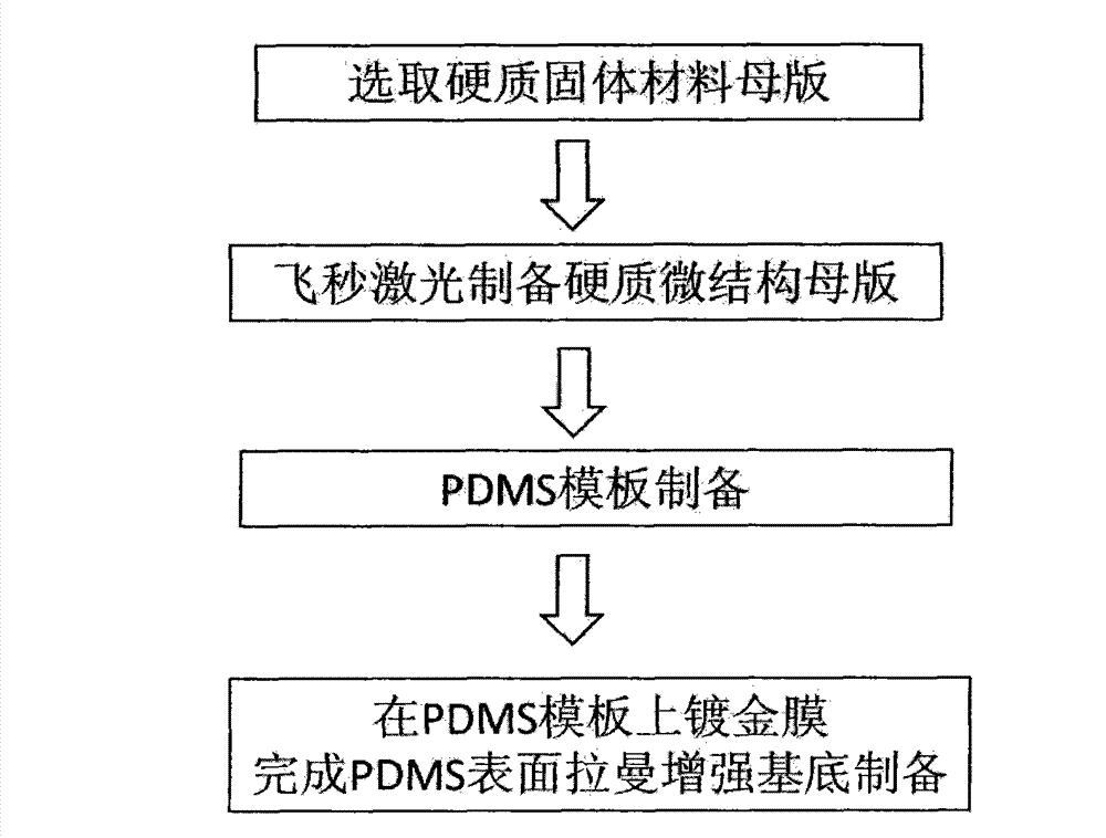
[0040] In the preparation method of the present invention, (1) choose a hard solid material as the master material, the hard solid material refers to a hard sheet or block material, and the material property can be a semiconductor material such as silicon, or a metal Materials such as copper, aluminum, etc., hard solid materials require flat surfaces, and the surface flatness means that the difference between the highest point and the lowest point on the surface of the material is less than or equal to 10 μm;

[0041] (2) Put the hard solid material into ethanol and acetone 1:1 mixed solution for ultrasonic cleaning for 15 minutes, then rinse with a large amount of deionized water to make the surface clean;

[0042] (3) The femtosecond laser irradiates the surface of the hard material to make a hard microstructure master;

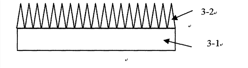
[0043] (4) Pouring liquid organic material polydimethylsiloxane (PDMS) on the surface of the processed hard microstructure master, so that PDMS covers the ...

Embodiment 1

[0052] The preparation method of PDMS surface enhanced Raman scattering substrate comprises the following steps:

[0053] 1. Select a silicon wafer with an n(110) resistivity of 2-10Ω*cm and a thickness of 400 μm as the hard master material.

[0054] 2. Ultrasonic clean the silicon wafer in ethanol, acetone 1:1 mixture for 15 minutes, and then rinse with a large amount of deionized water to make the surface clean.

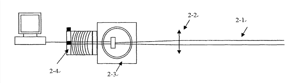
[0055] 3. Place the cleaned silicon wafer on the sample holder connected to the three-dimensional translation stage and fix it.

[0056] 4. Use a vacuum pump to evacuate the vacuum chamber, and then fill it with 0.6bar SF 6 gas, as a reactive gas.

[0057] 5. Adjust the incident femtosecond laser flux to 3kJ / m 2 .

[0058] 6. Through the control program, set the moving speed of the target piece to 1mm / s, and the row spacing to 100um, and perform surface scanning, and the scanning area is 3cm×3cm. After the scanning time is over, use a vacuum pump to remove the...

Embodiment 2

[0066] In order to detect the performance of the Raman-enhanced substrate on the PDMS surface, we add the step of measuring the Raman-enhanced substrate enhancement factor (EF) on the PDMS surface after step [6] in claim 1. The Raman-enhanced substrate on the PDMS surface is the substrate prepared in Example 1. The configuration concentration is 10 -1 M and 10 -6 M's R6G solution. drop by drop 10 -1 M R6G solution to the ordinary polished silicon surface, drop a drop of 10 -6 M R6G solution onto PDMS surface-enhanced Raman substrate. A Raman spectrometer from Renishaw Company was adopted, the magnification of the objective lens was 50×numerical aperture NA=0.5, the wavelength of the excitation light was 785 nm, and the integration time was 10 s.

[0067] EF=(I SERS ×N NR ) / (I NR ×N SERS )

[0068] where I SERS and N SERS Respectively represent the signal intensity of R6G Raman scattering on the SERS substrate and the number of molecules that the laser can irradiate...


PUM

PropertyMeasurementUnit
Thicknessaaaaaaaaaa
Thicknessaaaaaaaaaa

Abstract

The invention discloses a preparation method of a large-area surface enhancement raman scattering substrate. The preparation method comprises the following steps: at first, the surface of a hard solid material is irradiated by femtosecond laser to prepare a large-scale hard microstructural mother set; then, polydimethylsiloxane (PDMS) is poured on the hard microstructural mother set by the nanoimprint lithography technology, and the structure on the hard microstructural mother set is copied to prepare a PDMS framework; and finally, a gold film is plated on the PDMS framework to prepare the PDMS surface enhancement raman scattering substrate. The experiment results show that the preparation method has the advantages that the enhancement factors are high, enhancement factors in different positions of the substrate have good uniformity, the large-area surface enhancement raman scattering substrate can be prepared, the mother set can be repeatedly imprinted, the production cost is reduced, and in addition, god is taken as raman enhancement metal, so that the defect that silver is oxidized very easily is avoided.

Description

technical field [0001] The invention relates to the field of optical devices, in particular to a preparation of a large-area microstructure master by using a femtosecond laser, that is, embossing and replicating the microstructure of the master on a PDMS material, thereby making a large-area surface-enhanced Raman scattering substrate. The substrate can be applied to many fields such as nanofabrication, nanoimprint technology and biology. Background technique [0002] Raman scattering is the scattering of light frequency changes due to the interaction between incident light and molecules when light passes through a medium. From the Raman scattering spectrum, one can obtain the vibrational energy level information of the molecule. Since a specific vibration energy level corresponds to a specific chemical bond and molecular symmetry, the type of molecule can be determined through the vibration energy level, and Raman spectroscopy is also called "molecular fingerprint". In re...

Claims


Application Information

Patent Timeline
IPC IPC(8): G01N21/65
Inventor 吴强杨明齐继伟马寅星陈战东张心正孙骞许京军
Owner NANKAI UNIV
Why Eureka
Try Eureka