Method of forming resist pattern by nanoimprint lithography

a technology of nanoimprint lithography and resist pattern, which is applied in the direction of electric/magnetic/electromagnetic heating, instruments, photomechanical equipment, etc., can solve the problem of shortening the wavelength of light sources and requiring a new expensive exposure apparatus, and achieves the effect of superior etching resistan

Active Publication Date: 2009-07-30
TOKYO OHKA KOGYO CO LTD
View PDF4 Cites 36 Cited by
  • Summary
  • Abstract
  • Description
  • Claims
  • Application Information

AI Technical Summary

Benefits of technology

[0008]In the method of forming a resist pattern of the present invention using nanoimprint lithography, a resist pattern is formed by a bi-layer resist process using a chemically amplified negative resist composition containing a silsesquioxane resin (A), thereby providing superior etching resistance even in a case where a thin film is used.

Problems solved by technology

However, the shortening of wavelength of the light sources requires a new expensive exposure apparatus.

Method used


Image

  • Method of forming resist pattern by nanoimprint lithography
  • Method of forming resist pattern by nanoimprint lithography
  • Method of forming resist pattern by nanoimprint lithography

Examples


examples 1 to 3

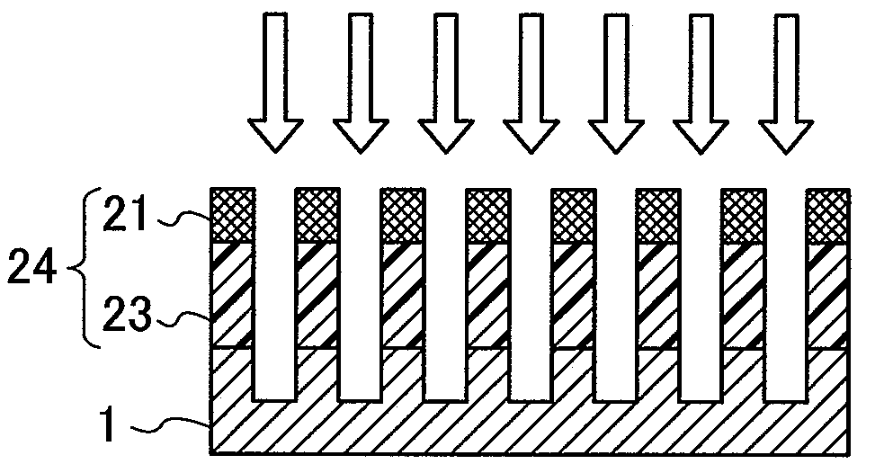
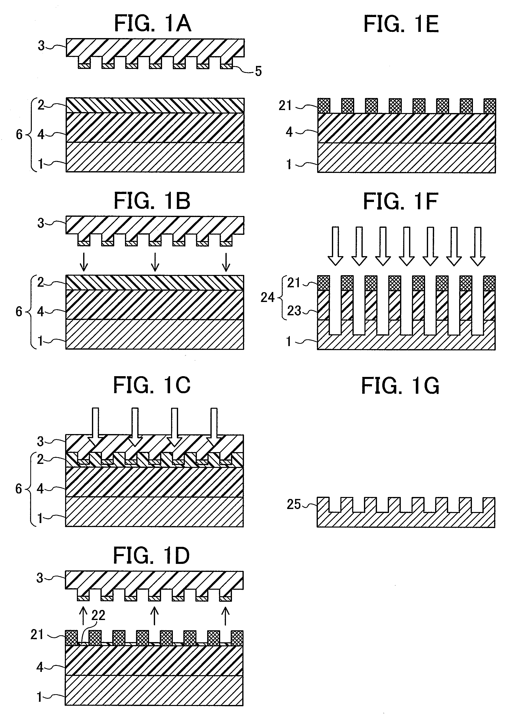
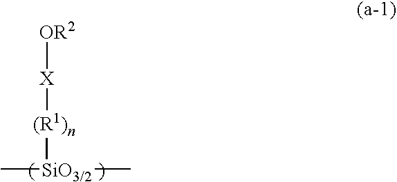
[0112]On an 8-inch silicon wafer on which a SiO2 film was formed, a material for forming organic film “TBLC-100” (manufactured by Tokyo Ohka Kogyo Co., Ltd.) was coated, and then baked on a hot plate at 230° C. for 90 seconds, thus forming an organic film of 250 nm in thickness. The chemically-amplified negative resist compositions of examples 1 to 3 shown in Table 1 were applied respectively onto the organic film, and dried by pre-baking (PAB) on a hot plate at 100° C. for 90 seconds, thus forming a resist film of 150 nm in thickness. Thereafter, a mold of light transmissive type, which is partially light-resistant by chrome, was pressed against the resist film, and a KrF excimer laser (248 mm) was irradiated thereon by a KrF exposure device NSR-S203. Subsequently, PEB (post exposure bake) at 110° C. was carried out for 90 seconds, and the mold was released. Then, development was performed at 23° C. for 60 seconds, using an aqueous tetramethylammonium hydroxide (TMAH) solution of 2...


PUM

PropertyMeasurementUnit
thicknessaaaaaaaaaa
temperatureaaaaaaaaaa

Abstract

A method of forming a resist pattern of high aspect ratio excelling in etching resistance by the use of nanoimprint lithography. The method of forming a resist pattern by nanoimprint lithography comprises the steps of disposing organic layer (4) on support (1); providing resist layer (2) on the organic layer (4) with the use of chemical amplification type negative resist composition containing silsesquioxane resin (A); pressing light transmission allowing mold (3) with partial light shielding portion (5) against the resist layer (2) and thereafter carrying out exposure from the upside of the mold (3); and detaching the mold (3).

Description

TECHNICAL FIELD[0001]The present invention relates to a method of forming a resist pattern by nanoimprint lithography. More particularly, the present invention relates to a method of forming a resist pattern using nanoimprint lithography, by forming a resist layer using a chemically amplified negative-type resist composition.BACKGROUND ART[0002]Lithography techniques have been used as a core technology in semiconductor device processes, and with recent advancement in highly integrated semiconductor integrated circuits (IC), exceedingly finer wiring patterns have been formed. Method of miniaturization are generally: use of a light source of shorter wavelength, such as shortening wavelength of light source using, for example, a KrF excimer laser, an ArF excimer laser, an F2 laser, an EUV (extreme ultraviolet) light, an EB (electron beam), or an X-ray; increasing numerical aperture (NA) of a lens of an exposure apparatus (increased NA); and the like. However, the shortening of waveleng...

Claims


Application Information

Patent Timeline
Patent Type & Authority Applications(United States)
IPC IPC(8): B29C59/16B81C99/00
CPCB82Y10/00B82Y40/00G03F7/0002G03F7/0382Y10S977/887B29C2035/0827B29C71/04B29C59/026B29K2085/00G03F7/0757
Inventor SATO, KAZUFUMIYAMADA, TOMOTAKA
Owner TOKYO OHKA KOGYO CO LTD
Why Eureka
Try Eureka