Negative plate as well as preparation method and application thereof
A technology of negative electrode sheet and layer activity, applied in the direction of negative electrode, battery electrode, active material electrode, etc., can solve the problems of serious volume expansion and rapid cycle decay of negative electrode sheet, reduce volume expansion rate, improve energy density, and improve capacity Effect
- Summary
- Abstract
- Description
- Claims
- Application Information
AI Technical Summary
Problems solved by technology
Method used
Image
Examples
Embodiment 1
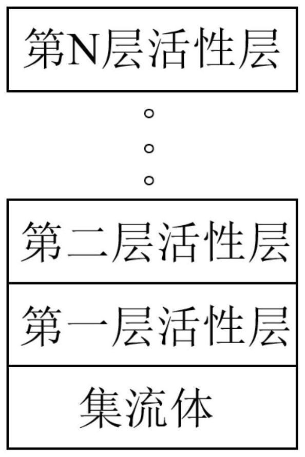
[0048] The structure of the negative plate provided in this embodiment is as follows: figure 1 As shown, N=2:
[0049] The first layer of active layer is obtained by coating 50 μm of the first layer of active layer slurry, and the first layer of active layer slurry includes 90g of pure nano-silicon and 10g of natural graphite;
[0050] The second active layer is obtained by coating 50 μm of the second active layer slurry, and the second active layer slurry includes 80 g of pure nano-silicon and 20 g of natural graphite.
[0051] The preparation method of the negative plate provided in this embodiment comprises:
[0052] 1. Weigh 90g of nano-silicon material and 10g of natural graphite, mix with 5g of binder PAA, 1g of dispersant sodium dodecylbenzenesulfonate, 2g of conductive agent carbon nanotubes, 2g of thickener CMC and 100g of water to prepare the first One layer of active layer slurry;
[0053] Weigh 80g of nano-silicon material and 20g of natural graphite, mix with 5...
Embodiment 2
[0057] The structure of the negative plate provided in this embodiment is as follows: figure 1 As shown, N=3:
[0058] The first layer of active layer is obtained by coating 40 μm of the first layer of active layer slurry, including 90g of pure nano-silicon and 10g of natural graphite in the first layer of active layer slurry;
[0059] The second layer of active layer is obtained by coating 30 μm of the second layer of active layer slurry, and the second layer of active layer slurry includes 80g of pure nano-silicon and 20g of natural graphite;
[0060] The third active layer is obtained by coating the slurry of the third active layer with a thickness of 30 μm, and the slurry of the third active layer includes 70 g of pure nano-silicon and 30 g of natural graphite.
[0061] The preparation method of the negative electrode sheet provided in this example is similar to that of Example 1, the only difference lies in the quality and coating thickness of pure nano-silicon and natur...
Embodiment 3
[0063] The structure of the negative plate provided in this embodiment is as follows: figure 1 As shown, N=4:
[0064] The first layer of active layer is obtained by coating 25 μm of the first layer of active layer slurry, including 90g of pure nano-silicon and 10g of natural graphite in the first layer of active layer slurry;
[0065] The second layer of active layer is obtained by coating 25 μm of the second layer of active layer slurry, and the second layer of active layer slurry includes 80g of pure nano-silicon and 20g of natural graphite;
[0066] The third layer of active layer is obtained by coating 25 μm of the third layer of active layer slurry, and the third layer of active layer slurry includes 70g of pure nano-silicon and 30g of natural graphite;
[0067] The fourth active layer is obtained by coating 25 μm of the fourth active layer slurry, and the fourth active layer slurry includes 60 g of pure nano-silicon and 40 g of natural graphite.
[0068] The preparati...
PUM
| Property | Measurement | Unit |
|---|---|---|
| Thickness | aaaaa | aaaaa |
| Thickness | aaaaa | aaaaa |
| Thickness | aaaaa | aaaaa |
Abstract
Description
Claims
Application Information

