

Semiconductor structure
A semiconductor and sidewall structure technology, applied in semiconductor devices, electrical components, circuits, etc., can solve problems such as semiconductor device damage, and achieve the effect of improving damage and relieving internal stress
- Summary
- Abstract
- Description
- Claims
- Application Information
AI Technical Summary
Problems solved by technology
Method used
Image

Examples
Embodiment 1
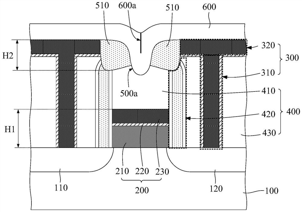
[0054] figure 1 It is a schematic diagram of the semiconductor structure in Embodiment 1 of the present invention, such as figure 1 As shown, the semiconductor structure includes:
[0055] A substrate 100, in which at least one semiconductor device and an interlayer dielectric layer 400 are formed, and the interlayer dielectric layer 400 covers the semiconductor device;
[0056] At least two interconnection structures 300, the interconnection structure 300 includes a contact plug 310 and a contact pad 320, the contact plug 310 penetrates the interlayer dielectric layer 400 and extends to the semiconductor device, the contact pad 320 covers the top of the contact plug 310 and extends to cover part of the top surface of the interlayer dielectric layer 400; and,
[0057] a groove between adjacent contact pads 320 of the bit line, the groove also extends downwards and stops in the interlayer dielectric layer 400; and,
[0058] an insulating filling layer filled in the groove, a...
Embodiment 2
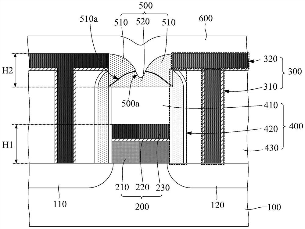
[0084] The difference from Embodiment 1 is that in this embodiment, the insulating filling layer further includes a second insulating portion covering the bottom of the groove.
[0085] figure 2 It is a schematic diagram of the semiconductor structure in Embodiment 2 of the present invention, such as figure 2 As shown, in this embodiment, the insulating filling layer 500 includes two first insulating parts 510 and a second insulating part 520, the first insulating part 510 covers the sidewall of the groove, and the second insulating part Portion 520 covers the bottom of the groove.
[0086] Further, a gap (that is, a first gap 510 a ) is formed between the second insulating portion 520 and the first insulating portion 510 , and the first gap between the first insulating portion 510 and the second insulating portion 520 510a extends toward the direction of the recess 500a from the corner where the bottom wall and the side wall of the groove connect to each other. Wherein, ...
Embodiment 3
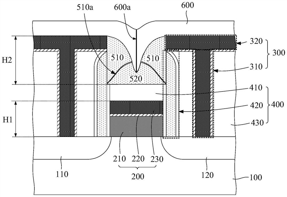
[0091] The difference from Embodiment 2 is that in this embodiment, the depth value H2 of the groove is greater than the height value H1 of the gate conductive layer, so that the groove has a larger aspect ratio and can be correspondingly The aspect ratio of the depression is increased, so that the portion of the covering layer corresponding to the depression can also form a void.
[0092] image 3 It is a schematic diagram of the semiconductor structure in Embodiment 3 of the present invention, such as image 3 As shown, in this embodiment, the depth of the groove extending downward in the shielding layer 410 in the height direction is lower, so that the depth value H2 of the groove is greater than the height value of the gate conductive layer H1, thereby making the groove The grooves have a larger aspect ratio.
[0093] Correspondingly, the recess 500a between the two first insulating parts 510 can have a larger aspect ratio. In this way, the portion of the covering layer...
PUM
 Abstract
Description
Claims
Application Information