Field plate, manufacturing method of semiconductor device and semiconductor device

A manufacturing method and semiconductor technology, applied in the fields of semiconductor devices, semiconductor/solid-state device manufacturing, electrical components, etc., can solve the problems of loss of oxide layer in the field area, high production cost, low withstand voltage reliability, etc., to ensure surface breakdown voltage, the effect of increasing the surface breakdown voltage

Active Publication Date: 2020-09-25
JOULWATT TECH INC LTD
View PDF8 Cites 1 Cited by
  • Summary
  • Abstract
  • Description
  • Claims
  • Application Information

AI Technical Summary

Problems solved by technology

[0003] In the traditional method, the thermal oxidation method is used to make the field plate oxide layer, and the thermal oxidation method only grows the oxide layer in the field area. If it is too thick, it will cause the loss of the field oxide layer in the subsequent etching process, making the traditional thermal oxidation metho

Method used


Image

  • Field plate, manufacturing method of semiconductor device and semiconductor device
  • Field plate, manufacturing method of semiconductor device and semiconductor device
  • Field plate, manufacturing method of semiconductor device and semiconductor device

Examples


Embodiment Construction

[0041] Various embodiments of the invention will be described in more detail below with reference to the accompanying drawings. In the various drawings, the same elements are denoted by the same or similar reference numerals. For the sake of clarity, various parts in the drawings have not been drawn to scale.

[0042] The specific implementation manners of the present invention will be further described in detail below in conjunction with the accompanying drawings and embodiments.

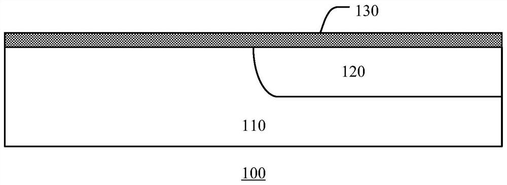
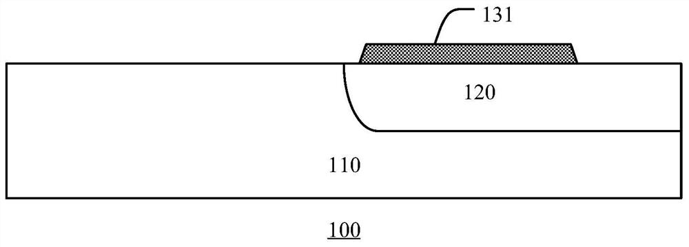
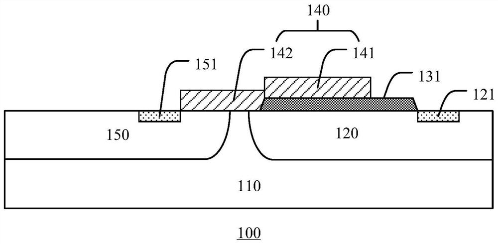
[0043] figure 1 , figure 2 and image 3 A schematic cross-sectional view of various stages of a method for fabricating a field plate oxide layer according to the prior art is shown. As shown in the figure, in this section, the field plate oxide layer 130 is located on the upper surface of the body region of the semiconductor device 100, and the body region includes the first body region 110 and the second body region located on the upper surface of the first body region 110, if An LDMOS (late...


PUM

PropertyMeasurementUnit
Thicknessaaaaaaaaaa

Abstract

The invention discloses a field plate, a manufacturing method of a semiconductor device and the semiconductor device. The manufacturing method of the semiconductor device comprises the manufacturing method of the field plate. The manufacturing method of the field plate comprises the step of manufacturing field plate oxide layers with different thicknesses by adopting TEOS deposition and high-temperature thermal annealing methods, so that the thickness of the field plate oxide layers can be increased under the condition of not causing surface silicon damage, and the voltage endurance capabilityof the device can be improved; the preparation of the field plate is completed by two steps of etching: firstly, performing dry etching and wet rinsing to obtain a middle-stage field plate structure,and then performing dry etching on the end part of the middle-stage field plate structure to obtain a final-stage field plate structure, so that the edge defect of the middle-stage field plate structure caused by wet rinsing is eliminated, and the voltage-withstanding reliability of a device is improved. The manufacturing method of the semiconductor device and the semiconductor device comprise the manufacturing method of the field plate, and a field plate oxide layer with a large thickness can be obtained, and the voltage withstanding is reliable.

Description

technical field [0001] The invention relates to the technical field of semiconductors, in particular to a method for manufacturing a field plate, a semiconductor device, and a semiconductor device. Background technique [0002] Field plate is a common terminal protection structure used to improve the resistance to high-voltage breakdown of semiconductor devices. In high-voltage devices, it is necessary to form a large-thickness field plate oxide layer under the polysilicon or metal field plate to reduce the vertical electric field intensity of the field plate terminal. , improve the breakdown voltage, and improve the withstand voltage reliability of the device. [0003] In the traditional method, the thermal oxidation method is used to make the field plate oxide layer, and the thermal oxidation method only grows the oxide layer in the field area. If it is too thick, it will cause the loss of the field oxide layer in the subsequent etching process, making the traditional ther...

Claims


Application Information

Patent Timeline
IPC IPC(8): H01L29/40H01L29/78H01L21/336
CPCH01L29/402H01L29/7816H01L29/66681
Inventor 陆阳
Owner JOULWATT TECH INC LTD
Why Eureka
Try Eureka