Optical structure for improving photoelectric conversion efficiency of silicon carbide photoconductive switch

A technology of photoelectric conversion efficiency and photoconductive switching, which is applied in the direction of circuits, electrical components, semiconductor devices, etc., to achieve the effect of increasing the optical distance

Pending Publication Date: 2020-10-02
NAT UNIV OF DEFENSE TECH
View PDF0 Cites 5 Cited by
  • Summary
  • Abstract
  • Description
  • Claims
  • Application Information

AI Technical Summary

Problems solved by technology

[0005] Increasing the laser power can increase the output current of the SiC photoconductive switch, but the actual high-po

Method used


Image

  • Optical structure for improving photoelectric conversion efficiency of silicon carbide photoconductive switch
  • Optical structure for improving photoelectric conversion efficiency of silicon carbide photoconductive switch
  • Optical structure for improving photoelectric conversion efficiency of silicon carbide photoconductive switch

Examples


Embodiment 1

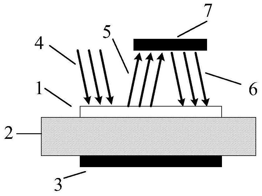
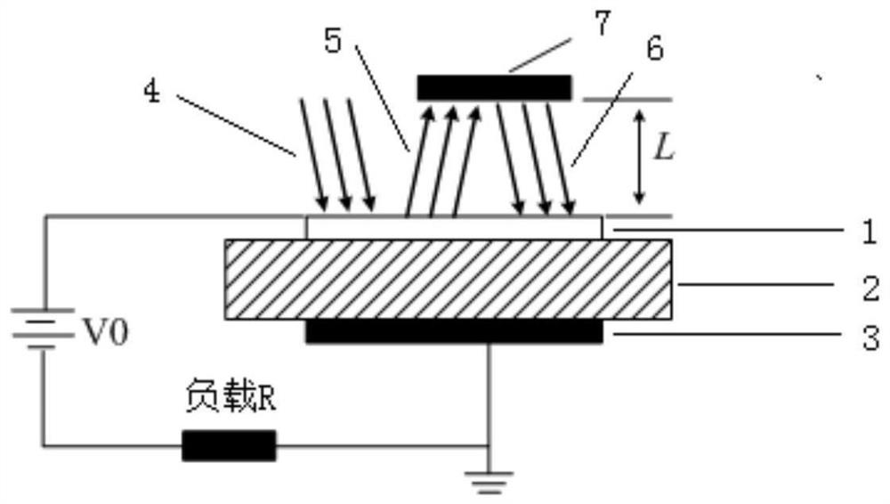
[0029] refer to figure 1 As shown, this embodiment provides an optical structure for improving the photoelectric conversion efficiency of a silicon carbide photoconductive switch, including: a silicon carbide photoconductive switch and a reflective structure 7; the silicon carbide photoconductive switch includes a transparent electrode 1 and a SiC material substrate 2 , the back-counter electrode 3 ; the transparent electrode 1 , the SiC material substrate 2 , and the back-counter electrode 3 are arranged sequentially from top to bottom; the reflective structure is located above the transparent electrode 1 .

[0030] Described reflective structure 7 is a kind of in metal film reflector, dielectric film reflector; Can adopt the reflector of the quartz substrate of metallized aluminum film, metal aluminum reflective film is easy to accomplish 90% to 532nm laser reflectivity; Can also The precious metal silver coating is used, and its reflectivity exceeds 95%; while the dielectri...

Embodiment 2

[0038] refer to Figure 4 As shown, according to the optical structure for improving the photoelectric conversion efficiency of the silicon carbide photoconductive switch described in Embodiment 1, the reflective structure 7 is also provided with a through-hole structure 8 to form a hollow reflective structure;

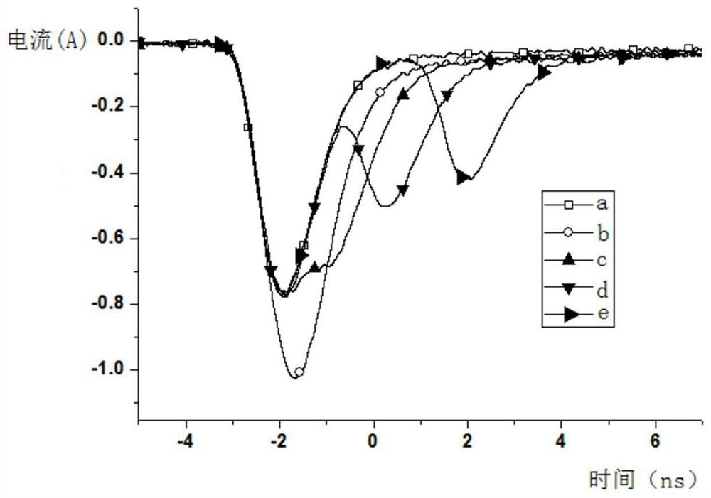
[0039] The aperture of the through-hole structure 8 is determined by the beam spot radius of the incident laser 4 and the optical damage threshold of the photoconductive switch material. Studies have shown that the SiC material of the transparent electrode 1 can withstand the peak power of light intensity of 10MW / cm 2 . The radius of the circular light spot in this embodiment is about 1 mm, therefore, the aperture used in the experiment of this embodiment is 1 mm; the thickness of the reflective structure 7 should be made thin enough to prevent the light beam from being incident on the surface of the light guide switch. The experiment of this embodiment uses The ref...

Embodiment 3

[0045] refer to Figure 6 As shown, according to the optical structure for improving the photoelectric conversion efficiency of the silicon carbide photoconductive switch described in the second embodiment, the through-hole structure 8 of the hollow reflection structure is provided with an optical fiber 9 to form an optical fiber fed into the hollow reflection structure. The optical fiber 9 is selected according to the actual application, and it is necessary to select an optical fiber capable of accommodating the pulse peak of the incident laser 4 without being damaged. In this embodiment, a multimode optical fiber is used, and the core diameter of the optical fiber is >100 um.

[0046] The specific working principle of the optical structure used to improve the photoelectric conversion efficiency of the silicon carbide photoconductive switch is:

[0047] The optical fiber 9 passes through the through-hole structure 8, irradiates the high-power laser pulse to the transparent el...


PUM

PropertyMeasurementUnit
Thicknessaaaaaaaaaa

Abstract

The invention discloses an optical structure for improving photoelectric conversion efficiency of a silicon carbide photoconductive switch. The optical structure comprises the silicon carbide photoconductive switch and a reflection structure. The silicon carbide photoconductive switch comprises a transparent electrode, a SiC material substrate and a back counter electrode, wherein the transparentelectrode, the SiC material substrate and the back counter electrode are sequentially arranged from top to bottom; the reflection structure is located above the transparent electrode; and the distanceL between the reflection structure and the transparent electrode satisfies L<ctau/4, wherein c represents the light speed in vacuum, and tau represents the full width at half maximum of the Gaussianlight pulse. According to the invention, an external optical structure is adopted to form an optical cavity structure, so that fed laser pulses are difficult to escape from the device; and laser pulseenergy which is not fully absorbed by the silicon carbide photoconductive switch and escapes is reflected into the device again, so that the absorption optical path of laser in the device is increased, and photoelectric response of the device can be ensured while high photoelectric conversion efficiency is realized.

Description

technical field [0001] The invention relates to the technical field of power electronics, in particular to an optical structure for improving the photoelectric conversion efficiency of a silicon carbide photoconductive switch. Background technique [0002] High-power switching devices are widely used in high-voltage power grids, radar detection systems, and network communications. They are the core components of power electronic systems and are developing in the direction of high power, high frequency, and integration. Photoconductive semiconductor switch (PCSS) is a new type of device formed by the combination of pulsed laser and optoelectronic semiconductor. It generates a large number of photogenerated carriers in the semiconductor device through fast laser pulses, controls the conductivity of the material, and realizes it by changing the intensity of the pulsed laser. To control the switch resistance, the switch is turned off and on by triggering and annihilating the pul...

Claims


Application Information

Patent Timeline
IPC IPC(8): H01L31/0232H01L31/0312H01L31/08
CPCH01L31/02327H01L31/0312H01L31/085
Inventor 王朗宁赵昱鑫楚旭荀涛杨汉武刘金亮贺军涛张军
Owner NAT UNIV OF DEFENSE TECH
Why Eureka
Try Eureka