Cleaning device for semiconductor product production and processing

A cleaning device and semiconductor technology, applied in the directions of dry gas arrangement, cleaning method using tools, cleaning method using liquid, etc., can solve the problems of time-consuming and laborious cleaning effect, etc., to improve processing efficiency and quality, simple operation, and practical sexual effect

Inactive Publication Date: 2020-10-09
顾骏
View PDF0 Cites 3 Cited by
  • Summary
  • Abstract
  • Description
  • Claims
  • Application Information

AI Technical Summary

Problems solved by technology

[0003] Particles such as silicon powder dust and metal dust are attached to the surface of semiconductor products during production and processing. Before subsequent processing, they need to be cleaned. The existing method is usually to manually hold a brush and dip it in cleaning solution while scrubbing. It is time-consuming and labor-intensive and the cleaning effect is poor at the same time. Therefore, the present invention proposes a cleaning device for the production and processing of semiconductor products to solve the above problems.

Method used


Image

  • Cleaning device for semiconductor product production and processing
  • Cleaning device for semiconductor product production and processing
  • Cleaning device for semiconductor product production and processing

Examples


Embodiment 1

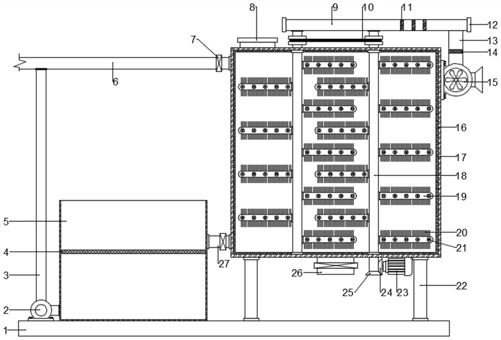
[0021] see figure 1 and figure 2 , in an embodiment of the present invention, a cleaning device for production and processing of semiconductor products includes a carrying base 1, a cleaning unit and a filtrate unit, the cleaning unit and the filtrate unit are both arranged on the carrying base 1, and the cleaning unit includes a cleaning box 16 and The brushing assembly, the brushing assembly is arranged in the cleaning box 16, the cleaning unit is used to clean the semiconductor products, and the filtrate unit is used to filter and purify the used cleaning solution and then transport it to the cleaning box 16 for practical use to achieve the purpose of recycling, and then Reduce production costs of enterprises.

[0022] The cleaning box 16 is fixed on the top of the bearing base 1 through a plurality of support rods 22. The top of the cleaning box 16 is provided with a product delivery port 8, and the bottom of the cleaning box 16 is provided with a product outlet 26 for t...

Embodiment 2

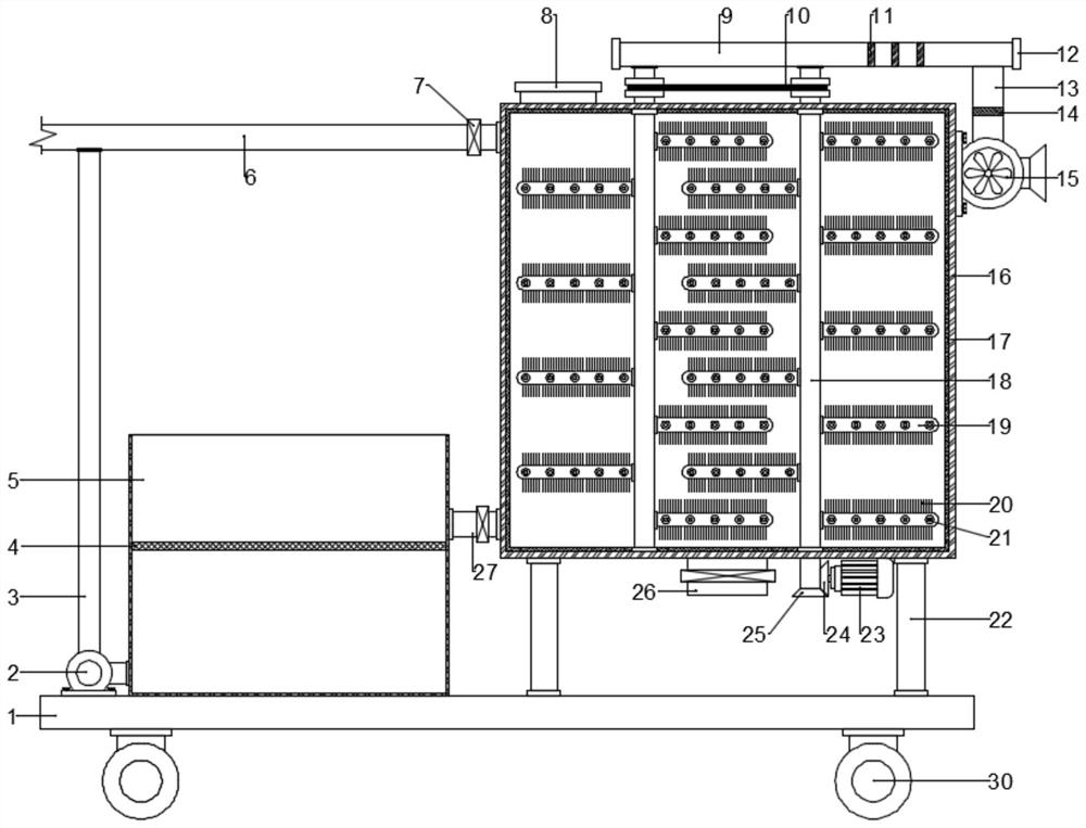
[0029] see image 3 The difference between the embodiment of the present invention and embodiment 1 is that, further, in order to facilitate the movement of the device, a plurality of moving wheels 30 are symmetrically arranged on the bottom of the bearing base 1, and the moving wheels 30 are self-locking rollers, and the staff The device can be easily and conveniently moved through the moving wheels 30, which is simple and trouble-free, convenient and practical.

[0030]The working principle of the present invention is: when the present invention is in use, first put the semiconductor product into the cleaning box 16 through the product delivery port 8, then open the liquid inlet valve 7 and inject an appropriate amount of cleaning liquid into the cleaning box 16, and then start the blower 15 and a servo motor 23, the servo motor 23 drives two rotating tubes 18 to rotate so that multiple turning tubes 19 stir the semiconductor product and make it squeeze and contact with mult...


PUM


Abstract

The invention discloses a cleaning device for semiconductor production and processing. The cleaning device comprises a bearing base, a cleaning unit and a liquid filtering unit. The cleaning unit andthe liquid filtering unit are both arranged on the bearing base. The cleaning unit comprises a cleaning tank and a scrubbing assembly. The scrubbing assembly is arranged in the cleaning tank. The cleaning device is reasonable in structure layout, easy to operate, convenient to use, capable of realizing mechanized cleaning of semiconductors and good in cleaning effect, has the rapid drying function, greatly improves the production and processing efficiency and quality of the semiconductors and has the great practicality.

Description

technical field [0001] The invention relates to the technical field of semiconductors, in particular to a cleaning device for semiconductor product production and processing. Background technique [0002] Semiconductor refers to a material whose conductivity is between that of a conductor and an insulator at room temperature. It is widely used in radios, televisions and temperature measurement. For example, a diode is a device made of a semiconductor. Whether it is from the perspective of technology or economic development From the point of view, the importance of semiconductors is very huge. Most of today’s electronic products, such as computers, mobile phones or digital recorders, have a very close relationship with the core units of semiconductors. Common semiconductor materials include silicon and germanium. , gallium arsenide, etc., and silicon is the most influential one in commercial applications among various semiconductor materials. [0003] Particles such as silic...

Claims


Application Information

Patent Timeline
IPC IPC(8): B08B3/10B08B1/04B08B13/00F26B21/00F26B25/04
CPCB08B3/10B08B3/102B08B13/00F26B11/14F26B21/001F26B21/004F26B25/04B08B1/32B08B1/12
Inventor 顾骏
Owner 顾骏
Why Eureka
Try Eureka