multi-die FPGA for realizing clock tree by using active silicon connection layer

A connection layer, multi-die technology, used in CAD circuit design, special data processing applications, climate sustainability, etc., can solve problems such as large structural limitations, asynchronous clocks, single signal interconnection, etc. Design Convergence, Improved Performance

Active Publication Date: 2020-10-09
WUXI ESIONTECH CO LTD
View PDF6 Cites 5 Cited by
  • Summary
  • Abstract
  • Description
  • Claims
  • Application Information

AI Technical Summary

Problems solved by technology

However, the above two patents are limited by the defects of the chip itself and the structural design. Both of them can only interconnect two adjacent IC dies arranged side by side, and can only realize signal interconnection in a single direction. Very limited
In addition, the balance of cross-die clock signals in this multi-die structure is also a problem that has to be considered, and it is also a big challenge. The conventional approach may be to connect the clock inputs between the die in series, but this It will cause the clock to be out of sync, and the clock skew will be very large, which will seriously affect the performance of cross-die design

Method used


Image

  • multi-die FPGA for realizing clock tree by using active silicon connection layer
  • multi-die FPGA for realizing clock tree by using active silicon connection layer
  • multi-die FPGA for realizing clock tree by using active silicon connection layer

Examples


Embodiment Construction

[0028] The specific embodiments of the present invention will be further described below with reference to the accompanying drawings.

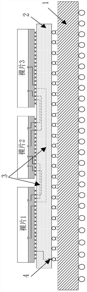
[0029] This application provides a multi-die FPGA that uses an active silicon connection layer to implement a clock tree. Please refer to figure 1 , the multi-die FPGA includes a substrate 1 , a silicon connection layer 2 and a number of FPGA die that are stacked at least sequentially from the bottom, which are respectively represented by die 1 , die 2 , etc., and so on. In actual implementation, the FPGA also includes an encapsulation shell that is packaged on the substrate 1, the silicon connection layer 2 and the outside of the FPGA die for protecting each component, and also includes pins connected to the substrate for signal extraction, etc., figure 1 These conventional structures are not shown in detail.

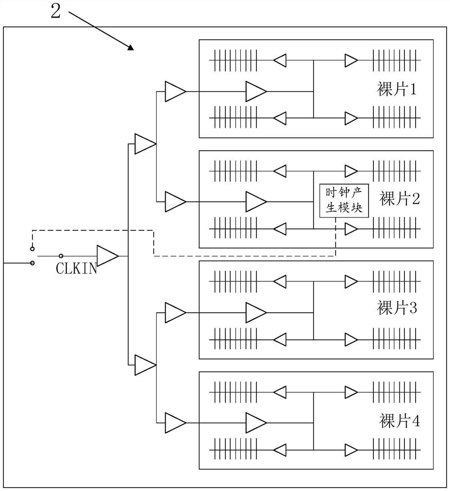
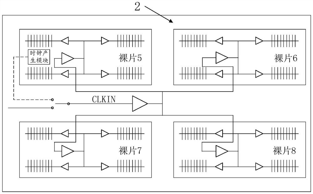
[0030] The FPGA of the present application does not use a single FPGA die structure, but includes multiple FPGA die, and the multipl...


PUM


Abstract

The invention discloses a multi-die FPGA for realizing a clock tree by using an active silicon connection layer. The multi-die FPGA comprises a plurality of FPGA dies, the plurality of FPGA dies are stacked on the same silicon connection layer, and interconnection communication is realized through cross-die connection lines in the silicon connection layer; active devices are also arranged in the silicon connection layer to construct a balance clock tree; a clock signal is pushed to each FPGA die through the balance clock tree; according to the multi-die FPGA and the manufacturing method thereof, the balance clock tree in the silicon connection layer can balance the time delay of the clock signal reaching each FPGA die, the problem that the clock skew is too large during cross-die communication is reduced, and the design convergence is accelerated, so that the performance of the multi-die FPGA is improved.

Description

technical field [0001] The invention relates to the technical field of semiconductors, in particular to a multi-die FPGA that utilizes an active silicon connection layer to realize a clock tree. Background technique [0002] FPGA (Field Programmable Gate Array, Field Programmable Logic Gate Array) is a hardware programmable logic device. It is not only used in mobile communication, data center and other fields, but also widely used in prototype verification in integrated circuit design, which can effectively verify The correctness of circuit function, while speeding up circuit design. Prototype verification needs to use the programmable logic resources inside FPGA to realize circuit design. With the continuous increase of the scale of integrated circuits and the realization of complex functions, the demand for the number of programmable logic resources of FPGA is constantly increasing. With the continuous increase, the number of FPGA programmable resources will become a gre...

Claims


Application Information

Patent Timeline
Patent Type & Authority Applications(China)
IPC IPC(8): G06F30/34
CPCG06F30/34Y02D10/00
Inventor 单悦尔徐彦峰范继聪张艳飞闫华
Owner WUXI ESIONTECH CO LTD
Why Eureka
Try Eureka