
CMOS device in BCD process and manufacturing method thereof

A manufacturing method and technology for MOS transistors, which are applied in semiconductor/solid-state device manufacturing, semiconductor devices, electrical components, etc., and can solve problems such as shortening the effective length of the device channel.

Active Publication Date: 2020-10-16
SHANGHAI HUAHONG GRACE SEMICON MFG CORP
View PDF6 Cites 2 Cited by
  • Summary
  • Abstract
  • Description
  • Claims
  • Application Information

AI Technical Summary

Problems solved by technology

With the continuous shortening of the device channel, the shortening of the effective length of the device channel caused by the introduction of LDD becomes non-negligible

Method used


Image

  • CMOS device in BCD process and manufacturing method thereof
  • CMOS device in BCD process and manufacturing method thereof
  • CMOS device in BCD process and manufacturing method thereof

Examples


no. 1 example B

[0078] The CMOS device in the BCD process of the first embodiment of the present invention:

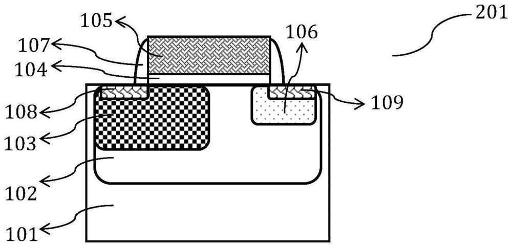
[0079] Such as figure 2 Shown is a schematic structural diagram of the first MOS transistor 201 of the CMOS device in the BCD process of the first embodiment of the present invention; the CMOS device and the LDMOS device in the BCD process of the first embodiment of the present invention are simultaneously integrated on the same semiconductor substrate 101 .

[0080] The CMOS device includes a first MOS transistor 201 whose channel conductivity type is the first conductivity type, and the LDMOS device includes a first LDMOS whose channel conductivity type is the second conductivity type. figure 2 In , the formation region of the first LDMOS is not shown.

[0081] The drift region of the first LDMOS is composed of the first doped region 103 doped with the second conductivity type. Since the formation region of the first LDMOS is not shown, the first doped region 103 constituting th...

no. 2 example B

[0097] The CMOS device in the BCD process of the second embodiment of the present invention:

Embodiment B

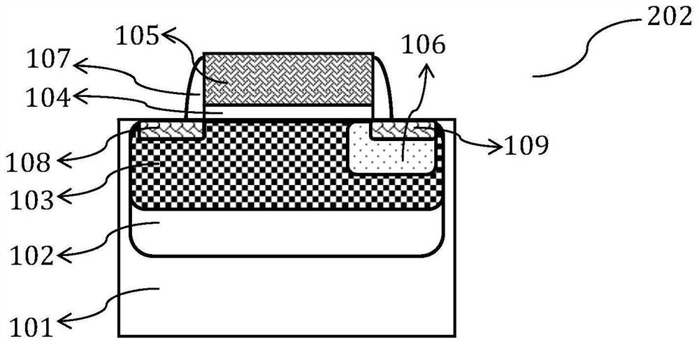
[0098] Such as image 3 As shown, it is a schematic structural diagram of the first MOS transistor 202 of the CMOS device in the BCD process of the second embodiment of the present invention; the difference between the CMOS device in the BCD process of the second embodiment of the present invention and the CMOS device in the BCD process of the second embodiment of the present invention where:

[0099] In the first MOS transistor 202, the first doped region 103 also extends to the first well region 102 outside the second side of the first gate structure and the first lightly doped Both the drain region 106 and the first drain region 109 are covered.

[0100] In the second MOS transistor, the second doped region also extends into the second well region outside the second side of the second gate structure and connects the second lightly doped drain region and Both the second drain regions are capped.


PUM


Abstract

The invention discloses a CMOS device in a BCD process. The CMOS device comprises a first MOS transistor with a channel conduction type of a first conduction type, and an LDMOS device comprises a first LDMOS with a channel conduction type of a second conduction type; a second conduction type doped first doped region is formed in a second conduction type first well region on the source region sideof the first MOS transistor, and the first doped region also forms a drift region of the first LDMOS. A first lightly doped drain region doped with the first conductivity type is formed in the first well region on the drain region side of the first MOS transistor. The first source region and the first drain region are formed on the surfaces of the first doped region and the first lightly doped drain region on the two sides of the first gate structure respectively. The invention further discloses a manufacturing method of the CMOS device in the BCD process. According to the invention, the high-voltage CMOS device can be realized, the short-channel effect of the device can be delayed, and the breakdown voltage of the device can be ensured without adding an additional process, so the size ofthe device can be further reduced, the conduction current is improved, and the conduction resistance is reduced.

Description

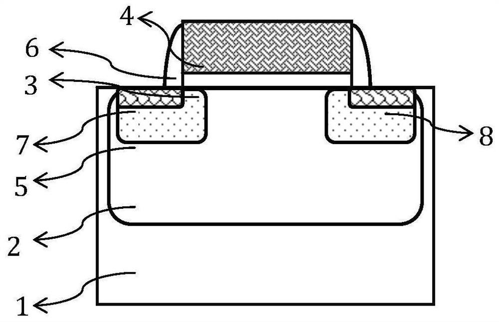
technical field [0001] The invention relates to the field of semiconductor integrated circuit manufacturing, in particular to a CMOS device in a BCD process. The invention also relates to a manufacturing method of the CMOS device in the BCD process. Background technique [0002] The BCD process is a bipolar transistor (Bipolar)-CMOS-DMOS process, which can simultaneously integrate bipolar transistors, CMOS and DMOS on a semiconductor substrate such as a silicon substrate. CMOS includes NMOS and PMOS, and DMOS includes LDMOS. [0003] Such as figure 1 Shown is a schematic structural diagram of a MOS transistor of a CMOS device in an existing BCD process. The MOS transistor includes NMOS and PMOS. Taking NMOS as an example, the MOS transistor includes: [0004] A P-type doped first well region 2, the first well region 2 is formed on a semiconductor substrate 1; usually, the semiconductor substrate 1 is a silicon substrate, and the doping type is P-type, and it can also be f...

Claims


Application Information

Patent Timeline
IPC IPC(8): H01L29/06H01L29/08H01L27/088H01L27/092H01L29/78H01L21/8238H01L21/336
CPCH01L27/088H01L27/092H01L29/7817H01L29/0684H01L29/0615H01L29/0847H01L29/0873H01L29/0882H01L21/823892H01L21/823814H01L29/66681
Inventor 许昭昭
Owner SHANGHAI HUAHONG GRACE SEMICON MFG CORP
Learn More