Phase shift photomask residual defect processing method and system and phase shift photomask
A phase-shift mask and defect processing technology, applied in the field of semiconductor manufacturing, can solve the problems of waste of production capacity and lengthy process of lithography machines
- Summary
- Abstract
- Description
- Claims
- Application Information
AI Technical Summary
Problems solved by technology
Method used
Image

Examples
no. 1 example
[0028] The embodiment of the present invention provides a phase-shift mask residual defect processing system, which can effectively solve the metal residue on the phase-shift layer, and can also avoid the waste of production capacity of the photolithography machine, reduce the time spent on defect processing, and shorten the time-consuming process flow .
[0029] The phase shift mask residual defect processing system provided in this embodiment includes a machine, a photoresist coater, a laser device, an etching device, a cleaning device, and a detection device, wherein the photoresist coater is used for the phase shift layer The photoresist layer is coated on the top; the laser equipment is used to partially expose the position corresponding to the defect on the photoresist layer; the etching equipment is used to partially etch the developed photoresist layer; the cleaning equipment is used to remove the photoresist layer. Resist layer; detection equipment is used to detect t...
no. 2 example
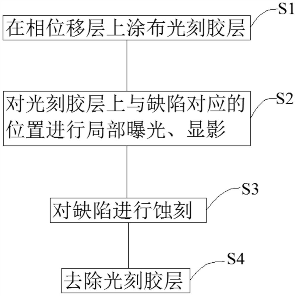
[0042] see Figure 1 to Figure 7 , the present embodiment provides a method for processing residual defects of a phase-shift mask, which is applicable to the system for processing residual defects of a phase-shift mask provided in the first embodiment, and the method includes the following steps:
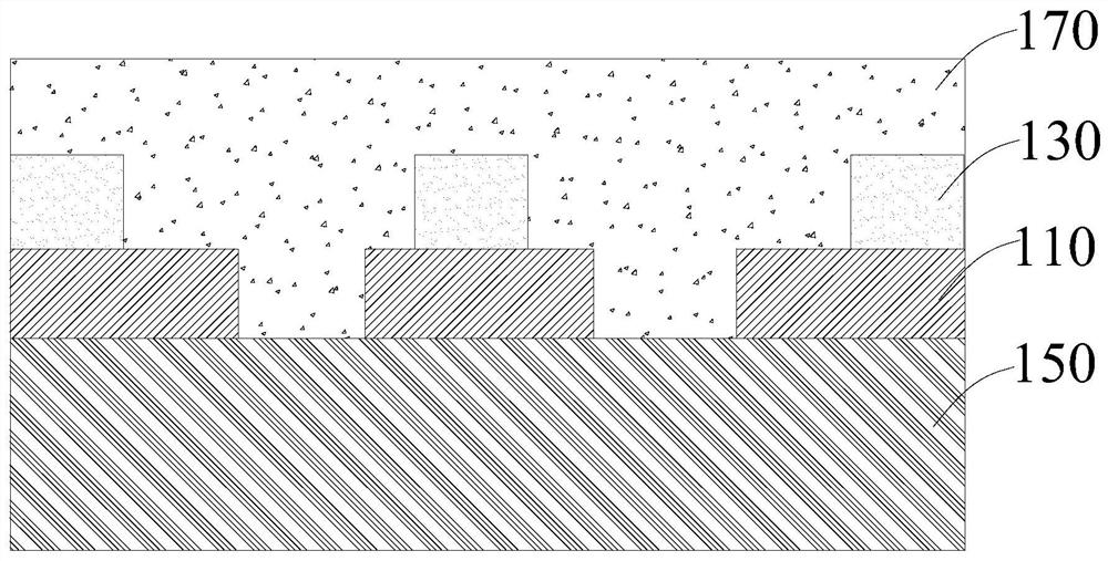
[0043] S1: Coating a photoresist layer 170 on the phase shift layer 110 .
[0044] Specifically, a photoresist is coated on the phase shift layer 110 of the phase shift mask 100 by using a photoresist coater, wherein the photoresist layer 170 is covered on the phase shift layer 110, and the photoresist layer 170 is formed. . The phase shift mask 100 includes a quartz plate 150, a phase shift layer 110 covering the surface of the quartz plate 150, and a chromium layer 130 covering the edge surface of the phase shift layer 110, wherein the phase shift layer 110 is generally silicon molybdenum. In this embodiment, the photoresist layer 170 covers the defect positions and the chromium...
no. 3 example
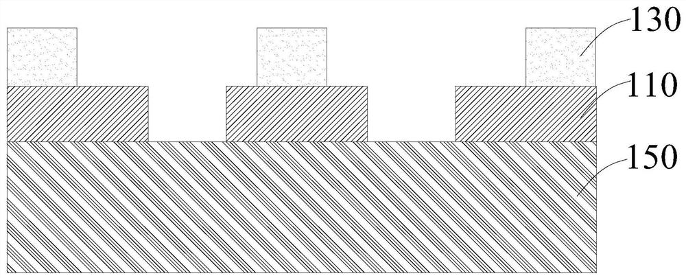
[0065] Please continue to see Figure 7 , the present embodiment provides a phase shift mask 100, which is manufactured after the method for treating residual defects in the phase shift mask provided in the second embodiment.
[0066] In this embodiment, the phase-shift mask 100 provided in this embodiment needs to be processed for the metal residual defects on the phase-shift layer 110 before shipment after being shaped by the manufacturing method. For the specific processing process, please refer to the second embodiment related content in the example.
[0067] The phase shift mask 100 provided in this embodiment includes a quartz plate 150, a phase shift layer 110, and a chromium layer 130. The phase shift layer 110 covers the surface of the quartz plate 150, and the chromium layer 130 covers the edge surface of the phase shift layer 110. The area of the displacement layer 110 not covered by the chromium layer 130 is provided with chip patterns expected to be replicated ...
PUM
 Abstract
Description
Claims
Application Information
 - R&D
- Intellectual Property
- Life Sciences
- Materials
- Tech Scout
- Unparalleled Data Quality
- Higher Quality Content
- 60% Fewer Hallucinations
Browse by: Latest US Patents, China's latest patents, Technical Efficacy Thesaurus, Application Domain, Technology Topic, Popular Technical Reports.
© 2025 PatSnap. All rights reserved.Legal|Privacy policy|Modern Slavery Act Transparency Statement|Sitemap|About US| Contact US: help@patsnap.com