Supercharge Your Innovation With Domain-Expert AI Agents!

Rapid turn-off RC-IGBT device with back double-MOS structure

A MOS structure and fast technology, applied in the semiconductor field, can solve the problems of long tail current, large voltage drop, and unsatisfactory breakdown voltage, etc.

Pending Publication Date: 2020-10-27
CHONGQING UNIV OF POSTS & TELECOMM
View PDF0 Cites 1 Cited by
  • Summary
  • Abstract
  • Description
  • Claims
  • Application Information

AI Technical Summary

Problems solved by technology

In the existing design, the freewheeling diodes of such devices are vertically integrated in the cell area, and the P-body in the cell area provides holes for the anode of the freewheeling diode, so the voltage drop above the P-type collector when it is turned off Larger, there are longer tail currents, unsatisfactory breakdown voltage BV, and turn-off loss E off or forward voltage drop V on Larger issues

Method used


Image

  • Rapid turn-off RC-IGBT device with back double-MOS structure
  • Rapid turn-off RC-IGBT device with back double-MOS structure
  • Rapid turn-off RC-IGBT device with back double-MOS structure

Examples


Embodiment 1

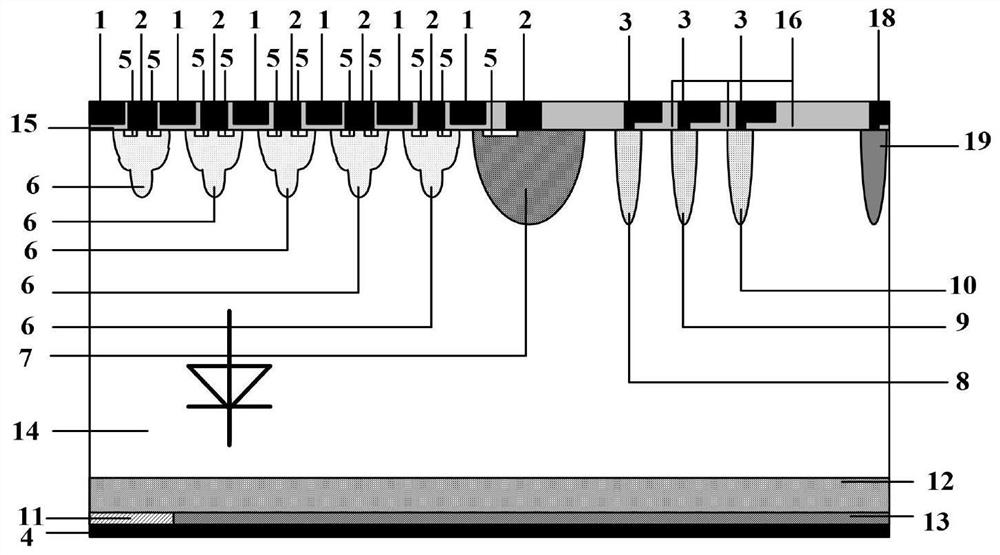
[0047] Such as Figure 6 As shown, a preferred embodiment of the present invention has a fast turn-off RC-IGBT device with a double MOS structure on the back, including a gate contact region 1, an emitter contact region 2, a metal field plate 3, a collector contact region 4, an emitter Pole 5, P-type well in cell region 6, P-type well in transition region 7, first field-limiting ring 8, second field-limiting ring 9, third field-limiting ring 10, N-type collector 11, N-type buffer layer 12 , P-type collector 13, N-type drift region 14, gate oxide layer 15, field oxide layer 16, collector oxide layer 17, field stop ring contact area 18, field stop ring 19, collector P-base 20;

[0048] The lower surface of the P-type collector 13 in the left, middle and right parts completely covers the upper surface of the collector contact region 4 . The left and right parts of the P-type collector 13 are doped silicon with a thickness of 2 μm, the middle concave part is doped silicon with a ...

Embodiment 2

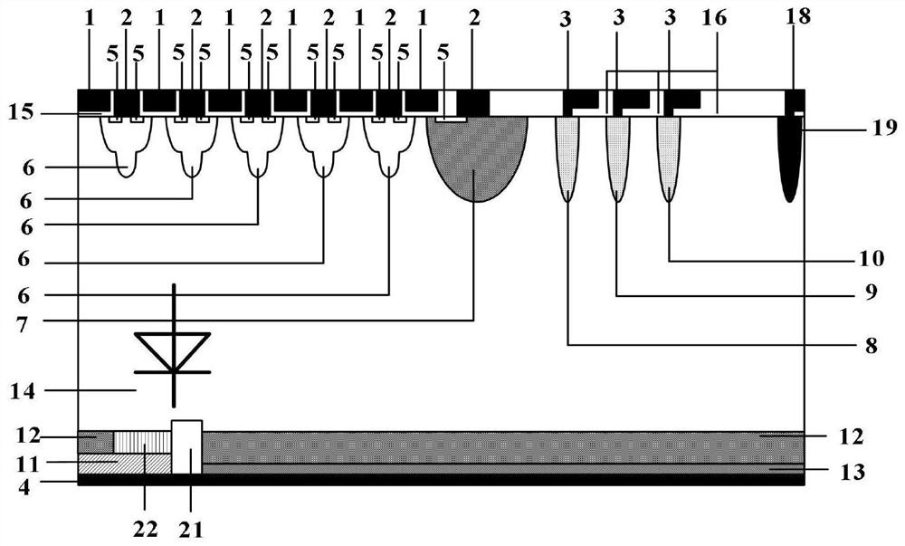
[0068] Such as Figure 7 As shown, the embodiment of the present invention preferably has a fast turn-off RC-IGBT device with a double MOS structure on the back. On the structure of Example 1, the silicon dioxide layer 17 of the MOS structure on the back is deep into the N-type buffer layer 12. At the same time, the collector metal contact region 4 and the P-type collector 13 part in the middle also penetrate into the N-type buffer layer 12, and the three keep the upper surface flush, and are located at the lower 0.5 μm of the N-type buffer layer 12. The N-type The surface of the buffer layer 12 is no longer concave, and the P-type collector in the middle part is 0.5 μm higher than the P-type collectors on both sides.

[0069] With the help of MEDICI simulation software, it is available for the provided figure 1 As shown in the traditional RC-IGBT, as Figure 5 The shown double anode type DARC-IGBT and the example proposed by the present invention are as Figure 6 The new ...


PUM

PropertyMeasurementUnit
Thicknessaaaaaaaaaa
Widthaaaaaaaaaa
Thicknessaaaaaaaaaa

Abstract

The invention relates to a rapid turn-off RC-IGBT device with a back double-MOS structure, and belongs to the technical field of semiconductors. The device comprises a gate contact region 1, an emitter contact region 2, a metal field plate 3, a collector contact region 4, an emitter 5, a cellular region P-type well 6,a transition region P-type well 7, a first field limiting ring 8, a second fieldlimiting ring 9, a third field limiting ring 10, an N-type collector 11, an N-type buffer layer 12, a P-type collector 13, an N-type drift region 14, a gate oxide layer 15, a field oxide layer 16, a collector oxide layer 17, a field stop ring contact region 18, a field stop ring 19 and a collector P-base 20. On the premise of ensuring elimination of the negative resistance effect during forward conduction, the device has relatively high turn-off speed, relatively low Von, good reverse conduction performance and voltage endurance capability of more than 600V, and the working stability and the current capability of the device are improved.

Description

technical field [0001] The invention belongs to the technical field of semiconductors and relates to a fast turn-off RC-IGBT device with double MOS structures on the back. Background technique [0002] Insulated Gate Bipolar Transistor (IGBT) is a composite fully controlled type composed of BJT (Bipolar Junction Transistor) bipolar transistor and MOSFET (Metal-Oxide-Semiconductor Field-Effect Transistor) insulated gate field effect transistor It is a voltage-driven power semiconductor device, so it has both the advantages of high input impedance of MOSFET and low conduction voltage drop of BJT. The IGBT combines the advantages of the above two devices, with low driving power and low saturation voltage. Therefore, it will become one of the core components of intelligent power integrated circuits and is widely used in home appliances, environmentally friendly automobiles and industrial production. It is a semiconductor power device with great potential in the future market. ...

Claims


Application Information

Patent Timeline
IPC IPC(8): H01L29/739H01L29/40H01L29/06H01L27/06
CPCH01L29/7393H01L29/402H01L29/0619H01L29/0684H01L27/0629
Inventor 陈伟中黄垚黄元熙李顺黄义贺利军张红升
Owner CHONGQING UNIV OF POSTS & TELECOMM
Features
  • R&D
  • Intellectual Property
  • Life Sciences
  • Materials
  • Tech Scout
  • Unparalleled Data Quality
  • Higher Quality Content
  • 60% Fewer Hallucinations
Learn More