Redox gridarene and synthesis method thereof, organic field effect transistor memory based on redox gridarene and preparation method thereof

A lattice aromatic hydrocarbon and memory technology, applied in the field of organic storage and information, can solve the problems of low storage density, high operating voltage, poor tolerance, etc., and achieve the effects of fast response operation, simple device structure, and cost reduction.

Active Publication Date: 2020-10-30
NANJING UNIV OF POSTS & TELECOMM
View PDF3 Cites 0 Cited by
  • Summary
  • Abstract
  • Description
  • Claims
  • Application Information

AI Technical Summary

Problems solved by technology

However, there are problems such as high operating voltage, slow reading and writing speed, poor tolerance, and unclear relationship between storage mechanism and molecular structure.
Nowadays, organic field effect transistors still face the following problems: (1) high operating voltage, slow reading and writing speed, poor device tolerance, low storage density, poor device stability (short maintenance time)
(2) The relationship between the storage mechanism and the molecular structure is not clear, and the storage performance also has a great dependence on the quality of the spin film. How to control the uniformity of the film quality, so as to stabilize the quality of the same batch of products; optimize the preparation process , cost reduction and other issues

Method used


Image

  • Redox gridarene and synthesis method thereof, organic field effect transistor memory based on redox gridarene and preparation method thereof
  • Redox gridarene and synthesis method thereof, organic field effect transistor memory based on redox gridarene and preparation method thereof
  • Redox gridarene and synthesis method thereof, organic field effect transistor memory based on redox gridarene and preparation method thereof

Examples


Embodiment 1

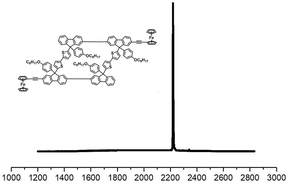
[0045] The redox lattice arene of the present embodiment, wherein X is S; K is 4-octyloxybenzene; G 1 , G 2 It is ferroceneacetylene, and its specific molecular formula is as follows:

[0046]

[0047] synthetic route:

[0048]

[0049] Specific preparation method:

[0050] A series of reactions shown in the above-mentioned synthetic route obtains bisbromogridine, bisbromogridine (0.5g / 0.26mmol) and ferroceneacetylene (0.16g / 0.77mmol) add catalyst Pd (PPh) under the protection of nitrogen 3 ) 4 (0.03g / 0.024mmol), CuI (0.03g / 0.16mmol) and put the reaction device in a light-proof environment, then add Et2N / DMF=3mL / 3mL with nitrogen gas for 2h to dissolve the reactant at room temperature, and then Add 3mol / L (KF / K 2 CO 3 ) 2mL, put it into a 90°C oil bath, heat and stir for 6h. The combined organic phases were extracted with dichloromethane, dried over anhydrous magnesium sulfate, filtered, and the solvent was removed with a rotary evaporator. The crude product was th...

Embodiment 2

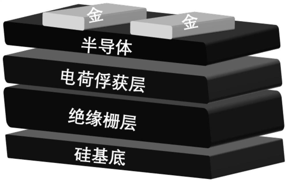
[0052] A kind of OFET memory structure of this embodiment, its structural diagram is as follows figure 1 ,include:

[0053] Heavy doped silicon substrate;

[0054] a gate electrode formed on the substrate;

[0055] a gate insulating layer covering the gate electrode;

[0056] a charge storage layer formed on the gate insulating layer;

[0057] an organic semiconductor layer formed on the charge storage layer; and

[0058] The source and drain electrodes on both sides of the channel on the surface of the organic semiconductor layer.

[0059] The substrate is generally made of highly doped silicon wafer, glass wafer or plastic PET.

[0060] In this embodiment, heavily doped silicon is used as the substrate and the gate electrode; silicon dioxide with a thickness of 50-300 nm is used as the gate insulating layer; the product compound 1 of Example 1 is used as the charge storage layer, and the thickness is 10-30 nm; A layer of pentacene with a thickness of 30-50nm is evapora...

Embodiment 3

[0062] In this embodiment, heavily doped silicon is used as the substrate and the gate electrode; 50 nm of silicon dioxide on the heavily doped silicon is used as the gate insulating layer; the product compound 1 of Example 1 is used as the charge storage layer, and its thickness is 20 nm, and then A layer of pentacene with a thickness of 50nm is vapor-deposited on the charge storage layer as an organic semiconductor layer; finally, gold is vapor-deposited on the semiconductor layer pentacene as a source-drain electrode.

[0063] During the experimental operation, the laboratory temperature was maintained at about 25°C and the humidity was 40%.

[0064] The memory of this embodiment, the specific preparation steps are as follows:

[0065] (1) Prepare redox lattice arene material solution, the solvent is selected as toluene, due to the solubility of redox lattice arene material, the redox lattice arene material and PS are blended at a mass ratio of 1:4 to obtain a blended mater...


PUM

PropertyMeasurementUnit
Thicknessaaaaaaaaaa
Thicknessaaaaaaaaaa
Thicknessaaaaaaaaaa

Abstract

The invention discloses redox gridarene, an organic field effect transistor memory based on the redox gridarene and a preparation method. The redox gridarene has a symmetrical geometric structure, hasobviously separated LUMO and HOMO energy levels, and has a structural formula shown in the specification. According to the invention, the redox gridarene is used as a charge storage layer of the organic field effect transistor memory. The memory can be used for manufacturing nonvolatile storage equipment, such as a mobile hard disk and a USB flash disk; and a flexible storage device, such as an electronic skin and a wearable device. The field effect memory device shows the advantages of being suitable for flexibility, large in area, low in process cost and the like of an organic memory. According to the invention, the memory is prepared through a simple process, and the preparation cost of the device is reduced. And the memory has great advantages in application.

Description

technical field [0001] The invention belongs to the field of organic storage and information technology, and specifically relates to redox lattice arene and its synthesis and the application of the lattice arene molecule in organic field effect transistor memory. Background technique [0002] As human society rapidly enters the Internet era, followed by the explosive growth of data, storage as the home of data is an indispensable element of information technology and artificial intelligence. This requires the memory to have faster read and write speed, smaller size, higher storage density and simpler manufacturing process. And it has the characteristics of flexibility, lightness and easy to carry. Non-volatile organic field effect transistor memory has the characteristics of fast storage speed and large storage capacity, and has low cost, low temperature and large-area inkjet printing processing, compatible with flexible substrates and easy integration, single transistor dr...

Claims


Application Information

Patent Timeline
IPC IPC(8): C07F17/02H01L51/05H01L51/30
CPCC07F17/02H10K85/331H10K10/46
Inventor 卞临沂张忍解蒙余洋解令海
Owner NANJING UNIV OF POSTS & TELECOMM
Why Eureka
Try Eureka