

Chip with composite layer and application of chip in biological detection
A biological detection and composite layer technology, applied in the direction of specific-purpose bioreactor/fermenter, microbial measurement/inspection, bioreactor/fermenter combination, etc., can solve the problems of large-scale, low-cost application gaps, etc.
- Summary
- Abstract
- Description
- Claims
- Application Information
AI Technical Summary
Problems solved by technology
Method used
Image

Examples
Embodiment 1
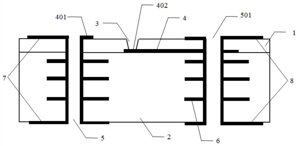
[0043] The chip structure of this embodiment is as figure 1 As shown, the first base layer 1 is located on the upper part of the chip, the first base layer 1 is a polyimide resin plate, and the thickness of the first base layer 1 is 0.1mm; the first base layer 1 is provided with hole electrodes, and the upper surface of the first base layer 1 A first blind hole 3 is provided. The first blind hole 3 is a circular hole with a diameter of 0.1 mm. The first blind hole 3 is formed by laser drilling technology. The bottom of the first blind hole 3 is provided with a metal circuit 4. A blind hole 3 and a metal line 4 form a hole electrode; the first electrode 401 is arranged near the upper end of the first metallized via hole 5, and the electrode 402 is arranged between the first base layer 1 and the second base layer 2, and covers the first blind hole. The entire bottom surface of the hole 3, the electrode 402 extends to the second metallized via hole 501; the second base layer 2 is...
Embodiment 2
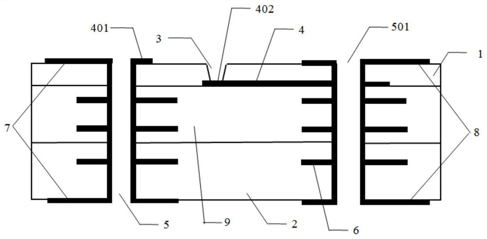
[0045] The chip structure of this embodiment is as figure 2 As shown, the first base layer 1 is located on the upper part of the chip, the first base layer 1 is a polyimide resin plate, and the thickness of the first base layer 1 is 0.1mm; the first base layer 1 is provided with hole electrodes, and the upper surface of the first base layer 1 A first blind hole 3 is provided. The first blind hole 3 is a circular hole with a diameter of 0.1 mm. The first blind hole 3 is formed by laser drilling technology. The bottom of the first blind hole 3 is provided with a metal circuit 4. A blind hole 3 and a metal line 4 form a hole electrode; the first electrode 401 is arranged near the upper end of the first metallized via hole 5, and the electrode 402 is arranged between the first base layer 1 and the third base layer 9, and covers the first blind hole. The entire bottom surface of the hole 3, the electrode 402 extends to the second metallized via hole 501; the third base layer 9 is ...
Embodiment 3
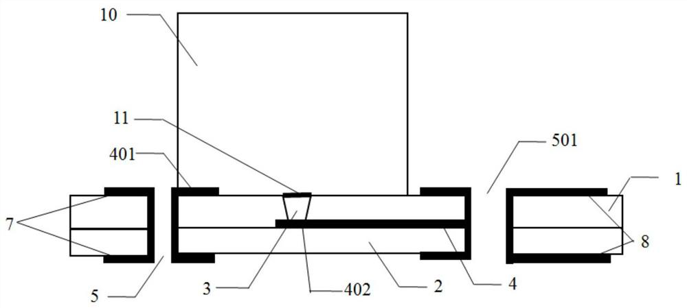
[0047] The structure of the chip applied in the nanopore gene sequencing device is as follows: image 3 As shown, the first base layer 1 is located on the top of the chip, the first base layer 1 is a polyimide resin board, and the thickness of the first base layer 1 is 0.1 mm. The upper part of the chip is provided with an electrolyte chamber 10, which is used to accommodate the electrolyte containing the DNA detection sample; the first base layer 1 is provided with a hole electrode, and the upper surface of the first base layer 1 is provided with a first blind hole 3, and the first blind hole 3 is a circular hole with a diameter of 0.1mm. The first blind hole 3 is formed by laser drilling technology. The bottom of the first blind hole 3 is provided with a metal circuit 4. The first blind hole 3 and the metal circuit 4 constitute a hole electrode. The first electrode 401 is arranged near the upper end of the first metallized via hole 5, the electrode 402 is arranged between th...
PUM
| Property | Measurement | Unit |
|---|---|---|
| pore size | aaaaa | aaaaa |
| thickness | aaaaa | aaaaa |
| thickness | aaaaa | aaaaa |
Abstract
Description
Claims
Application Information