

Semiconductor molybdenum target material and preparation method and application thereof
A semiconductor and molybdenum target technology, applied in the field of magnetron sputtering, can solve problems such as being unfavorable for large-scale promotion, cumbersome operation, and increasing production costs.
- Summary
- Abstract
- Description
- Claims
- Application Information
AI Technical Summary
Problems solved by technology
Method used
Image

Examples
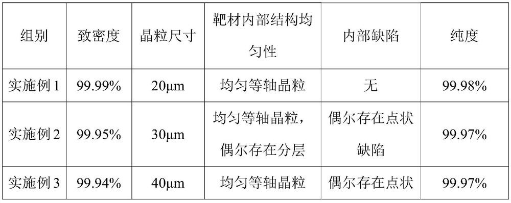
Embodiment 1
[0086] The present embodiment provides a kind of preparation method of semiconductor molybdenum target material, and described preparation method comprises the following steps:
[0087] (1) High-purity molybdenum powder screening and molding: the high-purity molybdenum powder with a purity of ≥99.5% is screened by a vibrating sieve machine to obtain a particle size of 180-200 mesh high-purity molybdenum powder, and the high-purity molybdenum powder is first Loading the rubber sleeve and binding it with a rubber band for sealing, then putting the sealed rubber sleeve into the steel sleeve, and then placing the steel sleeve in the cold isostatic pressing cylinder through the material rack to perform the cold isostatic pressing;
[0088] (2) cold isostatic pressing: the four-stage pressurization of described cold isostatic pressing comprises the following steps:
[0089] (a1) Increase the pressure to 15MPa at a pressurization rate of 0.5MPa / s, and hold the pressure for 5s;
[00...
Embodiment 2
[0117] This embodiment provides a method for preparing a semiconductor molybdenum target, except that the pressurization rate of the four-stage pressurization of the cold isostatic pressing described in step (2) is unified to 1.0MPa / s, and the pressure relief of the four-stage pressure relief The speed is uniformly 1.0MPa / s, and other conditions are identical to those in Example 1.
Embodiment 3
[0119] This embodiment provides a kind of preparation method of semiconductor molybdenum target material, except that the sintering described in step (3) is modified, other conditions are identical with embodiment 1, and specific content is as follows:
[0120] (3) Sintering: put the molybdenum target blank after cold isostatic pressing into a hydrogen protection sintering furnace, and adopt a step-by-step heating sintering method for sintering under a hydrogen atmosphere;
[0121] The heating stage at 20-1500°C includes 3 heating stages, and the heating rate gradually decreases from 2.56°C / min to 0.33°C / min, specifically including the following:
[0122] (c1) 20-710°C, heating rate 2.56°C / min, holding time 2h;
[0123] (c2) 710-1250°C, heating rate 1.67°C / min, holding time 3h;
[0124] (c3) 1250-1500°C, the heating rate is 0.33°C / min, that is, the time span of 20-1500°C is 27.5h, and the holding time at 1500°C is 5h;
[0125] The heating stage at 1500-1900°C includes 2 heat...
PUM
| Property | Measurement | Unit |
|---|---|---|
| density | aaaaa | aaaaa |
| density | aaaaa | aaaaa |
| particle size | aaaaa | aaaaa |
Abstract
Description
Claims
Application Information