Silicon-based magneto-optic isolator based on mode filter and preparation method

A mode filtering and filter technology, applied in the field of silicon-based optoelectronics integration, can solve the problems of lack of optical isolator integration methods and integration obstacles, and achieve the effect of high absorption loss and high isolation

Active Publication Date: 2020-10-30
INST OF SEMICONDUCTORS - CHINESE ACAD OF SCI +1
View PDF7 Cites 1 Cited by
  • Summary
  • Abstract
  • Description
  • Claims
  • Application Information

AI Technical Summary

Problems solved by technology

However, due to the lack of an effective and practical integration method for optical isolators, the integration of complex active devices on photonic integrated chips has also been hindered.

Method used


Image

  • Silicon-based magneto-optic isolator based on mode filter and preparation method
  • Silicon-based magneto-optic isolator based on mode filter and preparation method
  • Silicon-based magneto-optic isolator based on mode filter and preparation method

Examples


preparation example Construction

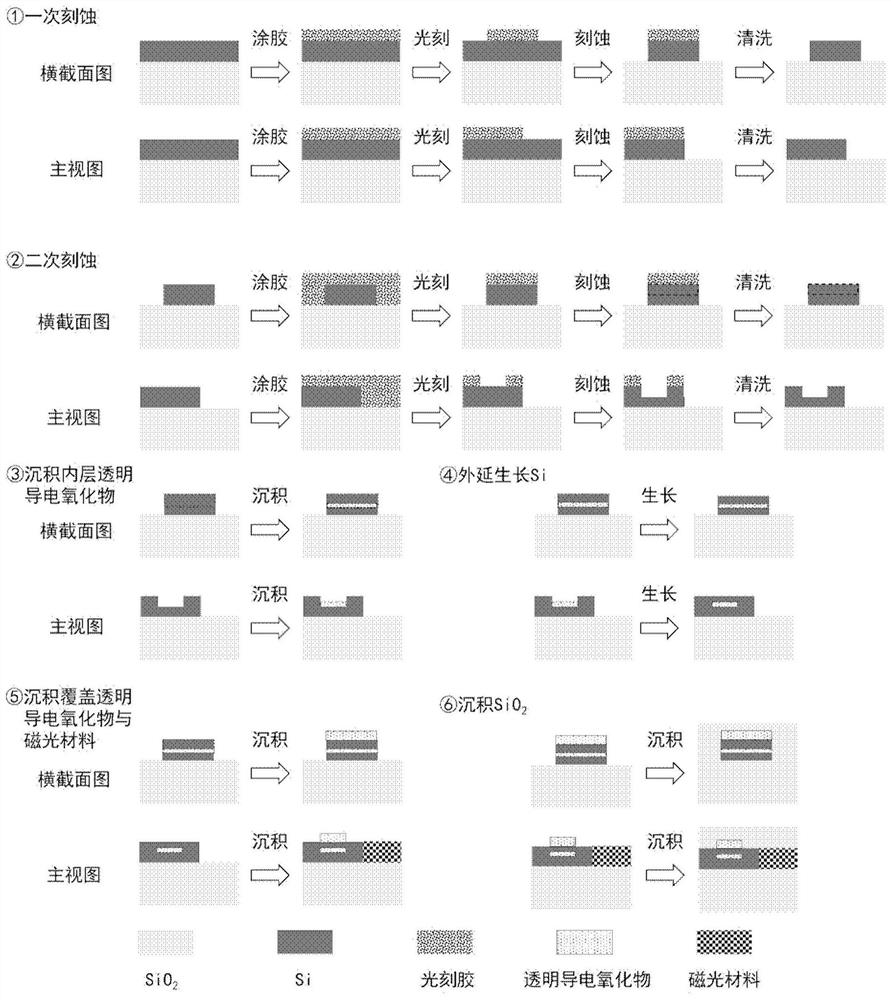
[0043] The invention also discloses a method for preparing a silicon-based magneto-optical isolator based on a mode filter, which includes the following steps:

[0044] Etching on SOI silicon wafer to form a strip-shaped silicon waveguide structure;

[0045] Forming the mode filter area through the secondary photolithography and etching process;

[0046] Depositing a transparent conductive oxide layer on the etched waveguide structure;

[0047] Epitaxially grow a layer of silicon film;

[0048] Depositing a transparent conductive oxide layer on the top layer of the mode filter area, and depositing an iron garnet film on the back end of the strip-shaped silicon waveguide structure to prepare a magneto-optical polarization Faraday rotator;

[0049] Deposit a layer of SiO 2 The thin film serves as the cladding layer on the device.

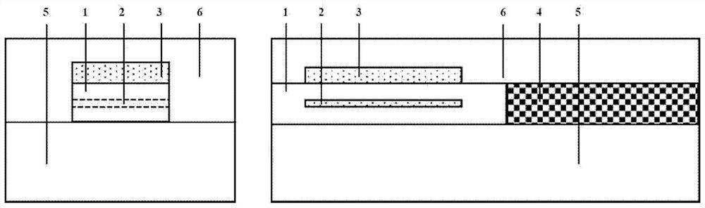
[0050] Preferably, the strip-shaped silicon waveguide is a rectangular waveguide;

[0051] Preferably, the strip-shaped silicon waveguide has a width of 400-2000 ...

Embodiment 1

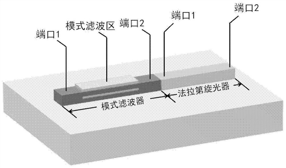
[0061] Such as figure 1 As shown, the present invention includes a mode filter and a Faraday rotator. The mode filter adopts a strip-shaped silicon waveguide structure embedded and covered with a transparent conductive oxide layer. The Faraday rotator adopts an iron garnet strip with a magneto-optical material doped with rare earth elements. The mode filter is divided into port 1 (ie the first port), the mode filter area, and port 2 (ie the second port) along the length direction; the Faraday rotator is divided into port 1 (ie the third port) along the length direction Port) and port 2 (ie the fourth port);

[0062] The input signal including the transverse electric field mode transmitted in the forward direction is input from port 1 of the mode filter. After entering the mode filter area, it is output from port 2 and enters port 1 of the Faraday rotator, which is implemented in the Faraday rotator. 45° polarization rotation is output from port 2; the reflected reverse transmissi...


PUM

PropertyMeasurementUnit
widthaaaaaaaaaa
thicknessaaaaaaaaaa
lengthaaaaaaaaaa

Abstract

The invention provides a silicon-based magneto-optic isolator based on a mode filter. The isolator comprises the mode filter and a Faraday rotator, the mode filter adopts a strip-shaped silicon waveguide structure embedded with a transparent conductive oxide layer, and the Faraday rotator adopts a strip-shaped magneto-optic material structure; an input signal of a transverse electric field mode transmitted in the forward direction is input from the mode filter, enters the Faraday rotator after passing through the mode filter area, and is output after 45-degree polarization rotation is achieved. Reflected reverse transmission light is input from the Faraday rotator, enters the Faraday rotator and continues to rotate by 45 degrees in the original direction, the reverse transmission light ischanged into a transverse magnetic field mode from the transverse electric field mode after rotating by 90 degrees in total, the reverse transmission light is lost by a transparent conductive oxide layer when entering the filter area of the mode filter, and therefore isolation of the reverse transmission light is achieved. The isolator provided by the invention has the characteristics of high isolation, low insertion loss, small device size, easy CMOS integration and the like.

Description

Technical field [0001] The invention relates to the technical field of silicon-based optoelectronics integration, in particular to a silicon-based magneto-optical isolator based on a mode filter. Background technique [0002] With the development of the information age, in order to better meet its "explosive growth" of information transmission needs, the performance requirements for optical fiber communication modules, links and systems are gradually increasing. In the optical path, due to various reasons, reflected light that is opposite to the forward transmission light direction will be generated. For example, when light is coupled into the optical fiber, due to the existence of connectors and fusion points, these end faces and points will be generated in the original transmission direction. Opposite reflected light. When the reflected wave photons return to the device, they perform a secondary interaction with the semiconductor material, which interferes with the normal carr...

Claims


Application Information

Patent Timeline
Patent Type & Authority Applications(China)
IPC IPC(8): G02F1/095G02B6/122G02B6/126G02B6/132G02B6/13
CPCG02B6/122G02B6/126G02B6/13G02B6/132G02F1/0955
Inventor 李明轩李金野于海洋戴双兴刘建国
Owner INST OF SEMICONDUCTORS - CHINESE ACAD OF SCI
Why Eureka
Try Eureka