Terahertz electromagnetic absorber based on metamaterial
An electromagnetic absorber and terahertz technology, applied in the field of terahertz electromagnetic absorbers, can solve the problems of insufficient absorption frequency band bandwidth, poor absorption performance, limited bandwidth, etc., and achieve superior absorption performance, improved absorption effect, and good robustness Effect
- Summary
- Abstract
- Description
- Claims
- Application Information
AI Technical Summary
Problems solved by technology
Method used
Image
Examples
Embodiment
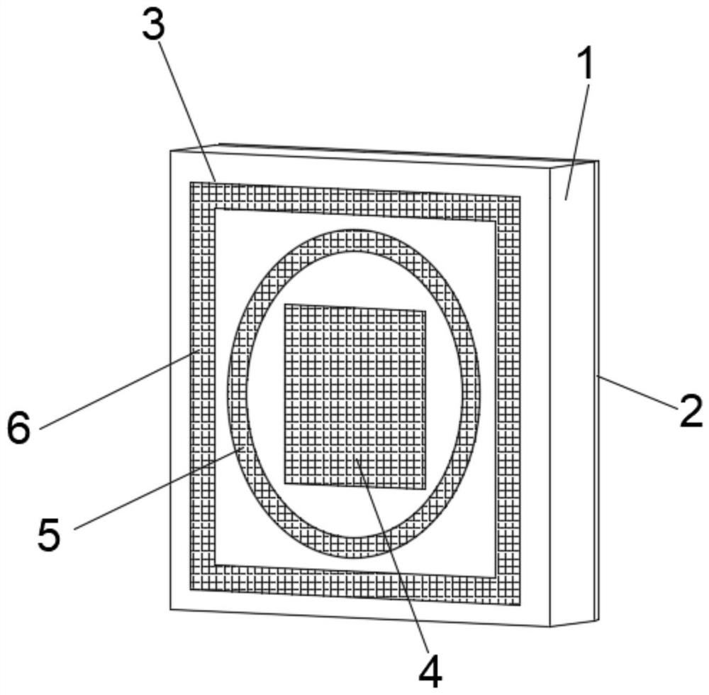
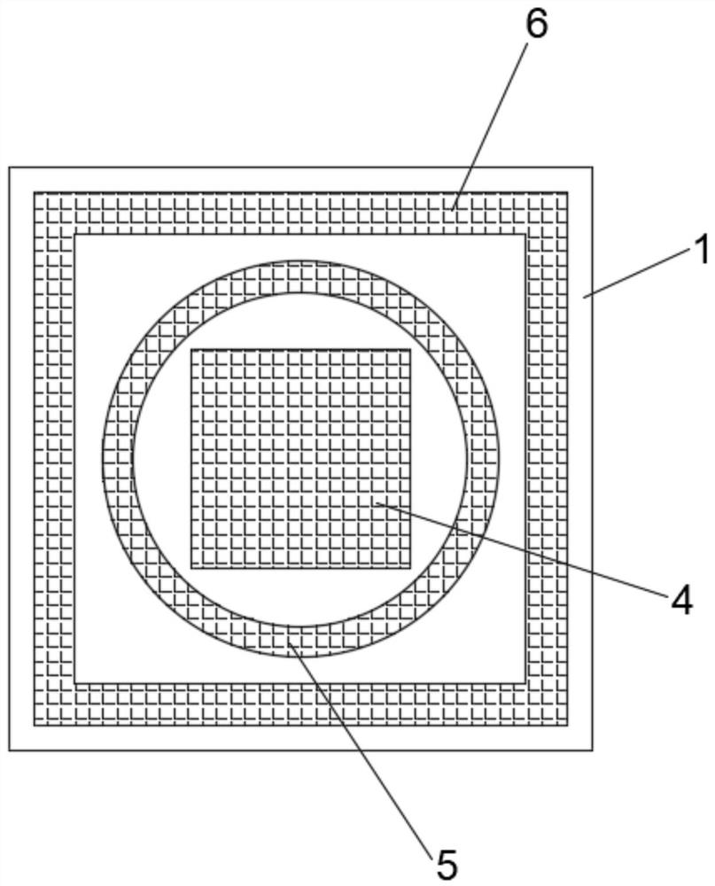
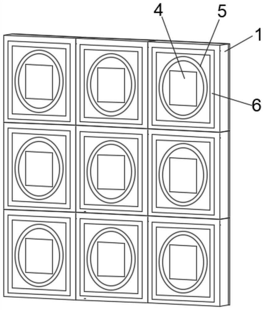
[0025] Embodiment: Terahertz electromagnetic absorbers based on metamaterials, such as Figure 1-2 As shown, it includes a dielectric layer 1 with a square cross section in the horizontal direction, the material of the dielectric layer 1 is glass material, the dielectric constant of the dielectric layer 1 is 4.41; the loss tangent angle of the dielectric layer 1 is 0.0004; the dielectric layer 1 has a length of 500 μm and a thickness of 80 μm; the bottom surface of the dielectric layer 1 is provided with an absorption bottom layer 2; the absorption bottom layer 2 has a length of 500 μm and a thickness of 0.2 μm, and is made of indium tin oxide; the dielectric layer 1 The surface is provided with a patch layer 3 made of indium tin oxide; indium tin oxide is ITO (Indium Tin Oxide), which is a material for n-type semiconductor coating processing. 780nm) as a transparent material, its light transmittance is as high as 90% in the visible light frequency band, it strongly reflects i...
Embodiment 2
[0036] Embodiment 2: on the basis of embodiment 1, as Figure 12 and Figure 13 As shown, the applicant is provided with a frame-shaped patch groove 7, an annular patch groove 8 and a square patch groove 9 on the dielectric layer 1; The surface of the dielectric layer is provided with a graphene layer 9, and the middle part of the four edges of the graphene layer 9 is respectively provided with a wave-shaped topological boundary 10; Resonant boundary 11; The four corners of the graphene layer 9 are respectively provided with a transmission hole lattice 12, and the transmission hole lattice 12 at each corner is in a regular triangular matrix shape; between the four described transmission hole lattices 12 An array grid 13 is formed. In the present invention, a frame-shaped patch groove, an annular patch groove and a square patch groove are arranged on the dielectric layer, and then a graphene layer is laid on the medium layer between the frame-shaped patch groove and the annul...
PUM
| Property | Measurement | Unit |
|---|---|---|
| Length | aaaaa | aaaaa |
| Thickness | aaaaa | aaaaa |
| Thickness | aaaaa | aaaaa |
Abstract
Description
Claims
Application Information


