Solar cell and preparation method thereof

A solar cell, amorphous silicon layer technology, applied in circuits, photovoltaic power generation, electrical components, etc., can solve problems such as unfavorable cell conversion efficiency and complex preparation process

Pending Publication Date: 2020-11-17
JINKO GREEN ENERGY SHANGHAI MANAGEMENT CO LTD +1
View PDF6 Cites 4 Cited by
  • Summary
  • Abstract
  • Description
  • Claims
  • Application Information

AI Technical Summary

Problems solved by technology

Therefore, the existing selective emitter structure manufacturing method is not conducive to improving the

Method used


Image

  • Solar cell and preparation method thereof
  • Solar cell and preparation method thereof
  • Solar cell and preparation method thereof

Examples


preparation example Construction

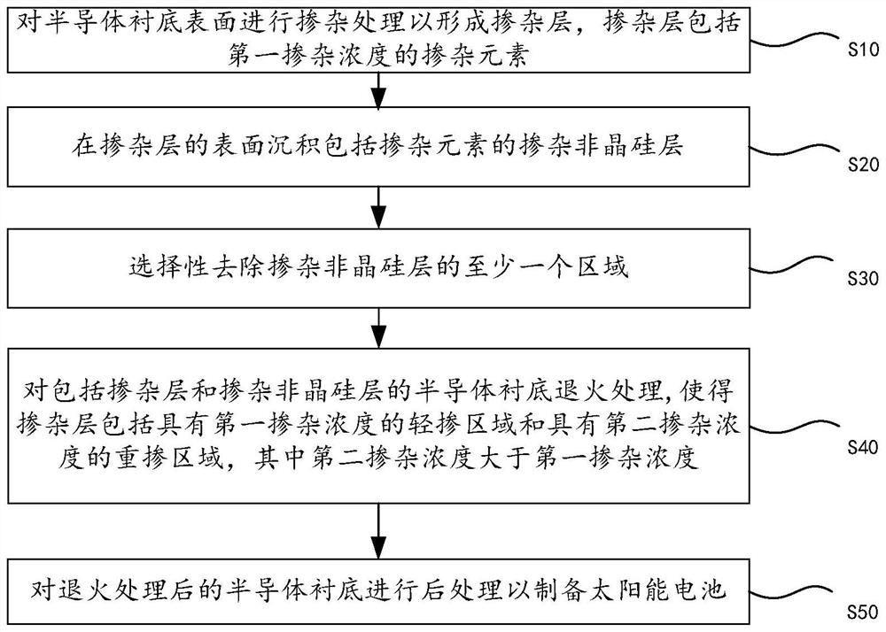
[0052] See figure 1 , figure 1 A flowchart of a method for preparing a solar cell provided in an embodiment of the present invention specifically includes the following steps:

[0053] Step S10 , performing doping treatment on the surface of the semiconductor substrate to form a doped layer, where the doped layer includes a doping element of a first doping concentration. Wherein, the formed doped layer may form a PN junction structure with the semiconductor substrate.

[0054] Specifically, an N-type or P-type doped layer may be formed on the surface of the semiconductor substrate by using any one or more methods of high temperature diffusion, slurry doping or ion implantation.

[0055] Exemplarily, taking the Topcon cell as an example, boron diffusion doping is performed on the front side (the surface facing the sun) of the N-type semiconductor substrate to form a P-type doped layer (P+ layer). Then deposit a boron-doped amorphous silicon layer on the surface of the P-type...

Embodiment approach

[0067] One-step deposition method: forming an amorphous silicon layer on the surface of the doped layer and simultaneously performing in-situ doping treatment to form the doped amorphous silicon layer; or,

[0068] Two-step deposition method: an amorphous silicon layer is deposited on the surface of the doped layer, and then the amorphous silicon layer is doped to form a doped amorphous silicon layer.

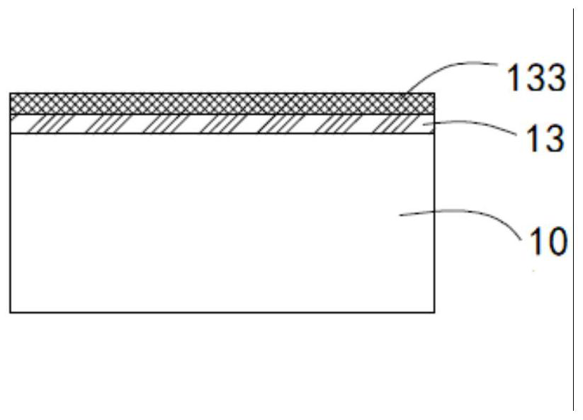
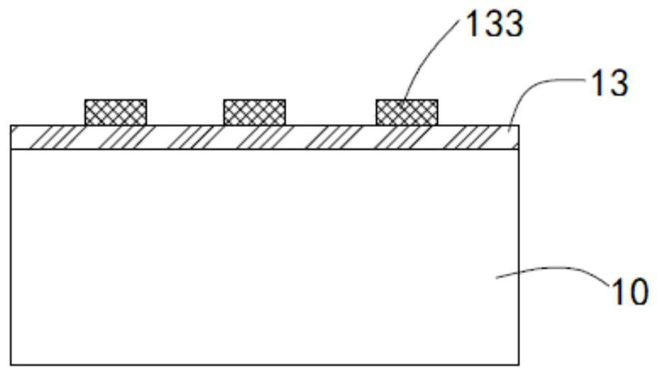
[0069] It should be noted that, if Figure 2a-2c As shown, the in-situ doped amorphous silicon is deposited on the surface of the doped layer 13, that is, the doped amorphous silicon layer 133 is formed by PEVCD or PVD, and the amorphous silicon layer is doped while depositing.

[0070] The doping process may also adopt any one or more methods of high temperature diffusion, slurry doping or ion implantation. The doped amorphous silicon layer 133 can be a P-type amorphous silicon layer, and its doping element can be three main group elements such as boron, gallium or indium; th...


PUM

PropertyMeasurementUnit
Thicknessaaaaaaaaaa
Thicknessaaaaaaaaaa

Abstract

The invention relates to the photovoltaic field, and provides a solar cell and a preparation method therefor, and the method comprises the following steps: carrying out the doping processing of the surface of a semiconductor substrate, so as to form a doping layer which comprises a doping element with a first doping concentration; depositing a doped amorphous silicon layer comprising doped elements on the surface of the doped layer; selectively removing at least one region of the doped amorphous silicon layer; annealing the semiconductor substrate including the doped layer and the doped amorphous silicon layer so that the doped layer includes a lightly doped region having a first doping concentration and a heavily doped region having a second doping concentration, wherein the second dopingconcentration is greater than the first doping concentration; and performing post-processing on the annealed semiconductor substrate to prepare the solar cell. According to the solar cell and the preparation method thereof, the preparation process of the solar cell is simplified, and the cell conversion efficiency is improved.

Description

technical field [0001] The present application relates to the technical field of photovoltaic cells, in particular, to a solar cell and a preparation method thereof. Background technique [0002] In order to improve the conversion efficiency of the solar cell, a selective emitter structure can be formed on the surface of the solar cell. At present, the selective emitter can be realized by laser doping, but the laser doping method is easy to damage the laser area and affect the efficiency of the battery; the selective emitter can also be formed by the reverse etching method, but the reverse etching method will destroy the front surface of the battery. The pyramid reduces its anti-reflection effect and affects the improvement of battery efficiency. Both the light expansion area and the re-expansion area of ​​the existing selective emitter structure are realized on the surface of crystalline silicon, the solid solubility of dopant atoms in crystalline silicon is low, and the c...

Claims


Application Information

Patent Timeline
IPC IPC(8): H01L31/20H01L31/0288H01L31/0352H01L31/068
CPCH01L31/202H01L31/208H01L31/0288H01L31/0682H01L31/035272Y02E10/547H01L31/1864H01L31/1804H01L31/068Y02P70/50H01L31/02167H01L31/022425H01L31/0747
Inventor 杨洁王钊郑霈霆张昕宇金浩
Owner JINKO GREEN ENERGY SHANGHAI MANAGEMENT CO LTD
Why Eureka
Try Eureka