Check patentability & draft patents in minutes with Patsnap Eureka AI!

GaN high-electron-mobility transistor structure and manufacturing method thereof

A technology of high electron mobility and fabrication method, applied in the field of GaN high electron mobility transistor structure and fabrication, can solve the problems of electric field concentration, affecting the performance and reliability of GaN high electron mobility transistor, etc.

Pending Publication Date: 2020-11-20
无锡先仁智芯微电子技术有限公司
View PDF4 Cites 2 Cited by
  • Summary
  • Abstract
  • Description
  • Claims
  • Application Information

AI Technical Summary

Problems solved by technology

[0003] Therefore, the technical problem to be solved by the present invention is to overcome the problem of electric field concentration in the prior art that the edge of the gate electrode is a sharp-angled structure, which will affect the performance and reliability of the GaN high electron mobility transistor, and provide a GaN high electron mobility transistor. High-rate transistor structure and its fabrication method

Method used


Image

  • GaN high-electron-mobility transistor structure and manufacturing method thereof
  • GaN high-electron-mobility transistor structure and manufacturing method thereof
  • GaN high-electron-mobility transistor structure and manufacturing method thereof

Examples


Embodiment 1

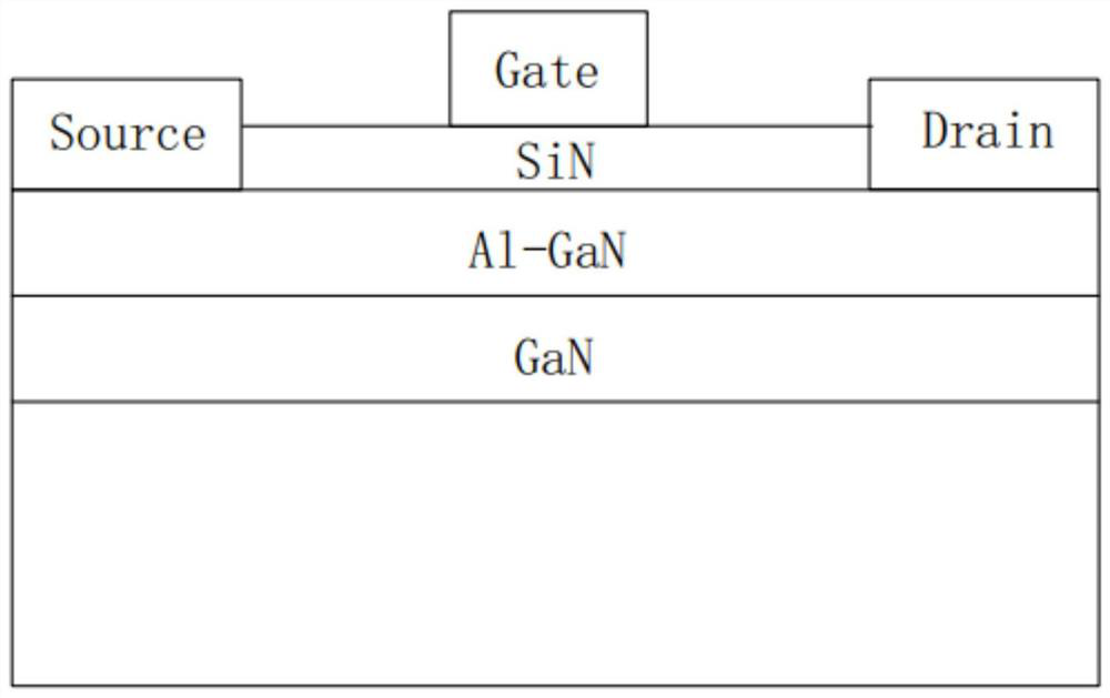
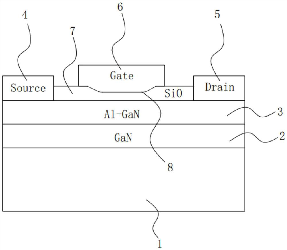
[0041] A GaN high electron mobility transistor structure such as figure 2 As shown, including a substrate 1, the material of the substrate 1 can be gallium nitride, silicon, sapphire, silicon carbide, aluminum nitride or other semiconductor materials; a channel layer 2 is grown on the substrate 1, and the channel layer 2 The material can be GaN; a barrier layer 3 is grown on the channel layer 2, and the material of the barrier layer 3 can be Al-GaN; a source 4, a drain 5 and a gate 6 are grown on the barrier layer 3, wherein the gate The electrode 6 is located between the source electrode 4 and the drain electrode 5. The source electrode 4, the drain electrode 5 and the gate electrode 6 are preferably a single-layer metal or a stack of multi-layer metals. The metal material can be Ti, Al, Ni, Au or Any one or more combinations of Mo; a dielectric layer 7 is grown between the gate 6 and the barrier layer 3, and a trench 8 is formed on the dielectric layer 7 at least along the ...

Embodiment 2

[0046] A GaN high electron mobility transistor structure such as Figure 6 As shown, including a substrate 1, the material of the substrate 1 can be gallium nitride, silicon, sapphire, silicon carbide, aluminum nitride or other semiconductor materials; a channel layer 2 is grown on the substrate 1, and the channel layer 2 The material can be GaN; a barrier layer 3 is grown on the channel layer 2, and the material of the barrier layer 3 can be Al-GaN; a source 4, a drain 5 and a gate 6 are grown on the barrier layer 3, wherein the gate The electrode 6 is located between the source electrode 4 and the drain electrode 5. The source electrode 4, the drain electrode 5 and the gate electrode 6 are preferably a single-layer metal or a stack of multi-layer metals. The metal material can be Ti, Al, Ni, Au or Any one or more combinations of Mo; a dielectric layer 7 is grown between the gate 6 and the barrier layer 3, and a trench 8 is formed on the dielectric layer 7 at least along the ...

Embodiment 3

[0051] A method for fabricating a GaN high electron mobility transistor structure, such as Figure 7 shown, including the following steps:

[0052] S1. A substrate 1 is provided.

[0053] Wherein, the substrate 1 may be one or more combinations of sapphire, silicon carbide, silicon, lithium niobate, silicon-on-insulator substrate, gallium nitride or aluminum nitride.

[0054] S2 , forming a channel layer 2 on the substrate 1 .

[0055] The channel layer 2 provides a channel for carrier movement. In this embodiment of the present invention, the channel layer 2 is unintentionally doped GaN.

[0056] S3 , forming a barrier layer 3 on the channel layer 2 .

[0057] The potential barrier layer 3 acts as a potential barrier, preventing the carriers in the channel layer 2 from flowing to the barrier layer 3. In this embodiment of the present invention, the barrier layer 3 is Al-GaN that is not intentionally doped.

[0058] S4, forming a dielectric layer 7 on the barrier layer 3, ...


PUM


Abstract

The invention relates to the technical field of electronic part manufacturing, in particular to a GaN high-electron-mobility transistor structure and a manufacturing method thereof, and aims to solvethe problem that in the prior art, due to the fact that the edge of a gate electrode is of a sharp corner structure, an electric field is concentrated, and the performance and reliability of a GaN high-electron-mobility transistor can be affected. The GaN-based high-electron-mobility transistor structure is technically characterized by comprising a substrate; a channel layer positioned on the substrate; a barrier layer located on the channel layer; a source electrode, a drain electrode and a grid electrode located on the barrier layer, and a dielectric layer positioned between the grid electrode and the barrier layer. The grid electrode is located between the source electrode and the drain electrode; a groove is formed in the dielectric layer in the gate width direction, and the edge, corresponding to the gate, of the groove is a circular bead. The stress concentration effect of the gate edge is overcome by removing the sharp corners at the gate edge, so that the breakdown voltage ofthe GaN high-electron-mobility transistor is further improved, and the performance of the high-electron-mobility transistor is further improved.

Description

technical field [0001] The invention relates to the technical field of electronic component manufacturing, in particular to a GaN high electron mobility transistor structure and a manufacturing method thereof. Background technique [0002] Today, silicon-based power electronic devices occupy the mainstream consumer market. However, with the continuous development of technology, the potential of Si materials in achieving higher withstand voltage, lower on-resistance and higher switching speed has been exhausted. The band gap of GaN is about 3 times that of Si, the critical breakdown field strength is also 1 order of magnitude higher than that of Si, and the electron mobility and thermal conductivity are also better, which makes GaN-based high electron mobility transistors in power conversion, microwave It has obvious advantages in high-voltage, high-current, high-frequency and high-temperature workplaces such as communications. A large number of researchers have proposed va...

Claims


Application Information

Patent Timeline
Patent Type & Authority Applications(China)
IPC IPC(8): H01L29/778H01L29/423H01L21/335
CPCH01L29/7786H01L29/42316H01L29/66462
Inventor 不公告发明人
Owner 无锡先仁智芯微电子技术有限公司
Features
  • R&D
  • Intellectual Property
  • Life Sciences
  • Materials
  • Tech Scout
  • Unparalleled Data Quality
  • Higher Quality Content
  • 60% Fewer Hallucinations
Learn More