Copper metaaluminate memristor based on flexible substrate and preparation method

A flexible substrate and memristor technology, applied in the direction of electrical components, etc., to achieve the effect of simple preparation process

Pending Publication Date: 2020-11-20
UNIV OF ELECTRONIC SCI & TECH OF CHINA
View PDF7 Cites 3 Cited by
  • Summary
  • Abstract
  • Description
  • Claims
  • Application Information

AI Technical Summary

Problems solved by technology

However, so far there are few reports on copper met

Method used


Image

  • Copper metaaluminate memristor based on flexible substrate and preparation method

Examples


Example Embodiment

[0030] Example 1

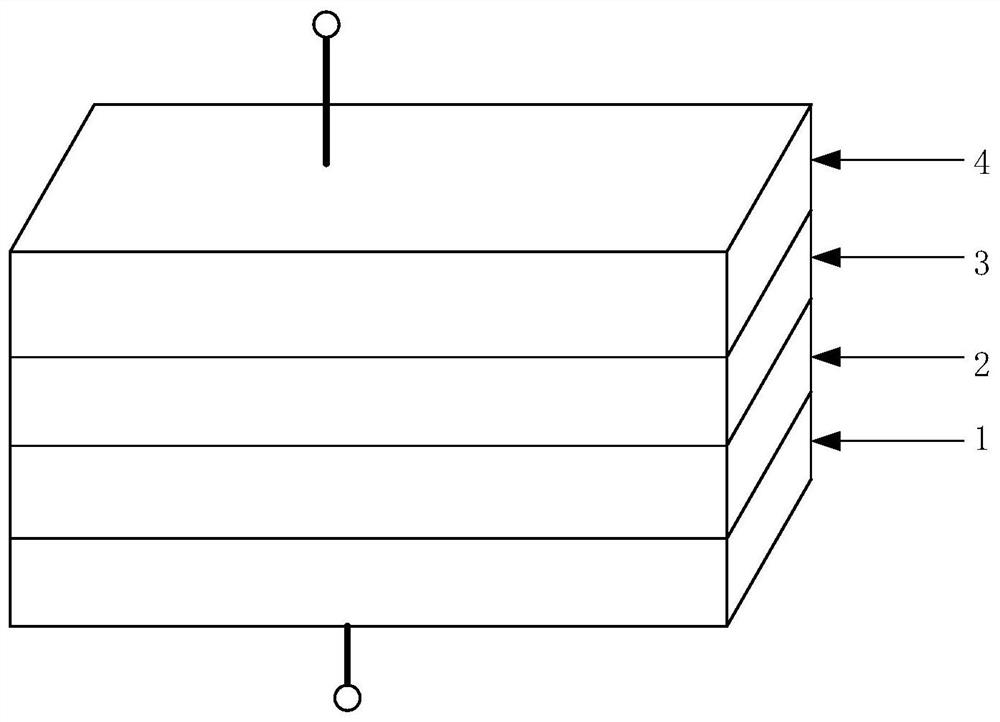
[0031] This embodiment provides a copper metaaluminate memristor based on a flexible substrate. The memristor has a vertical four-layer structure of an upper electrode 4, a resistive layer 3, a lower electrode 2, and a flexible substrate 1 from top to bottom. The upper electrode 4 of the memristor is a copper film; the resistive layer 3 of the memristive device is a copper metaaluminate film; the lower electrode 2 is a transparent conductive film of indium tin oxide; the flexible substrate of the memristor 1 is polyethylene naphthalate.

[0032] The resistive change layer 3 of the memristor is obtained by radio frequency sputtering, and has a thickness of 50 nm to 300 nm.

[0033] The bottom electrode 2 is an indium tin oxide bottom electrode with a thickness of 100-200 nm.

[0034] This embodiment also provides a method for preparing a copper metaaluminate memristor based on a flexible substrate, which includes the following process steps:

[0035] (1) Prepare poly...

Example Embodiment

[0048] Example 2

[0049] This embodiment provides a copper metaaluminate memristor based on a flexible substrate. The memristor has a vertical four-layer structure of an upper electrode 4, a resistive layer 3, a lower electrode 2, and a flexible substrate 1 from top to bottom. The upper electrode 4 of the memristor is a copper film or a silver film; the resistive layer 3 of the memristive device is a copper metaaluminate film; the lower electrode 2 is a transparent conductive film of indium tin oxide; the memristor The flexible substrate 1 is made of polyethylene terephthalate material.

[0050] The resistive change layer 3 of the memristor is obtained by radio frequency sputtering, and has a thickness of 50 nm to 300 nm.

[0051] The upper electrode 4 of the memristor is a copper film.

[0052] The bottom electrode 2 is an indium tin oxide bottom electrode with a thickness of 100-200 nm.

[0053] This embodiment also provides a method for preparing a copper metaaluminate memristor b...


PUM

PropertyMeasurementUnit
Thicknessaaaaaaaaaa
Thicknessaaaaaaaaaa

Abstract

The invention provides a copper metaaluminate memristor based on a flexible substrate. The memristor is sequentially provided with an upper electrode, a resistive layer, a lower electrode and a vertical four-layer structure of the flexible substrate from top to bottom. An upper electrode of the memristor is a copper film or a silver film; a resistive layer of the memristor is a copper metaaluminate film; and the lower electrode is an indium tin oxide transparent conductive film. The flexible substrate is polyethylene naphthalate or polyethylene glycol terephthalate mateiral. According to the flexible memristor based on the copper metaaluminate thin film, the preparation process is simple, the cost is low, and good resistance change characteristics can be obtained on the polymer flexible substrate. According to the memristor, the material system of the resistive layer of the memristor is widened, and the memristor is expected to be applied to the fields of flexible devices and wearableelectronic devices.

Description

technical field [0001] The invention belongs to the field of semiconductor optoelectronic devices, in particular to a copper metaaluminate memristor based on a flexible substrate and a preparation method thereof. Background technique [0002] As the fourth basic circuit element after resistors, capacitors, and inductors, memristors have the characteristics of simple device structure, fast working speed, and low power consumption. They have important application prospects in information storage, logic operations, and neuromorphic chips. The memristor has a sandwich structure of "electrode / resistive layer / electrode", and its resistive switching characteristics are closely related to electrode materials and resistive switching materials. To a certain extent, the resistance-switching characteristics exhibited by memristors determine its application fields. In order to meet different application scenarios, researchers have adopted various methods to obtain different resistive sw...

Claims


Application Information

Patent Timeline
IPC IPC(8): H01L45/00
CPCH10N70/801H10N70/24H10N70/8836H10N70/011
Inventor 李伟伊海田伟陈鹏宇李东阳李春梅蒋向东
Owner UNIV OF ELECTRONIC SCI & TECH OF CHINA
Why Eureka
Try Eureka