Eureka AIR delivers breakthrough ideas for toughest innovation challenges, trusted by R&D personnel around the world.

Preparation method of metal material surface deformation layer transmission electron microscope sample

A technology for transmission electron microscope samples and metal materials, which is applied in the field of metal material transmission electron microscope sample preparation, can solve the problems of low cost and difficulty in preparing metal material surface deformation layer transmission electron microscope samples by electrochemical double-spraying method, and achieves low cost and excellent preparation process. Ease of use and high efficiency

Active Publication Date: 2020-11-24
ANHUI UNIVERSITY OF TECHNOLOGY AND SCIENCE
View PDF11 Cites 0 Cited by
  • Summary
  • Abstract
  • Description
  • Claims
  • Application Information

AI Technical Summary

Problems solved by technology

[0003] In view of the above-mentioned defects, the present invention provides a method for preparing a transmission electron microscope sample of a deformed layer on the surface of a metal material, which solves the problem that it is difficult to prepare a transmission electron microscope sample of a deformed layer on the surface of a metal material by the electrochemical double-spray method, and effectively ensures that the double-spray thinning area is generated in the material In surface deformation, the preparation process of this method is simple and easy, with high efficiency and low cost

Method used


Image

  • Preparation method of metal material surface deformation layer transmission electron microscope sample
  • Preparation method of metal material surface deformation layer transmission electron microscope sample

Examples


Embodiment 1

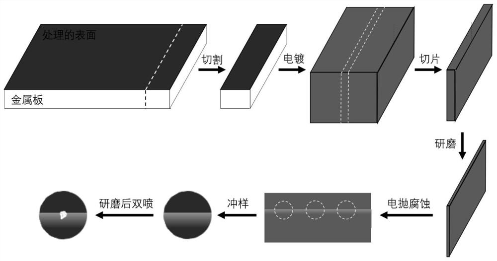
[0023] (1) From the pure copper plate after surface treatment, cut 10x10mm squares by wire cutting, and carry out alkali cleaning and pickling activation treatment;

[0024] (2) Place the activated square sample in the electroplating pool to electroplate the outer cladding layer. The electroplating solution formula is CuSO4 aqueous solution, the Cu2+ concentration is about 80g / ml, and the pH value is about 4; the pure copper plate is used as the anode plate , Constant current control, current density 35mA / cm2, electroplating at room temperature, electromagnetic stirring.

[0025] (3) Cutting and grinding: wire electric discharge cutting is adopted, perpendicular to the treatment surface, and the thickness is 1mm. Sandpaper was used to mechanically grind to a thickness of 60 μm.

[0026] (4) Electrochemical polishing and corrosion of the electroplating interface: Use pointed stainless steel tweezers to hold the ground thin slice sample, connect the tweezers to the positive pol...

Embodiment 2

[0032] (1) From the surface-treated copper-aluminum alloy (Cu-11w.t.%Al) plate, cut 8x8mm squares by wire cutting, and carry out alkali cleaning and pickling activation treatment;

[0033] (2) the square sample after the activation is placed in the electroplating pool, and the outer cladding layer is electroplated; the electroplating solution formula is CuSO4 aqueous solution, Cu2 + concentration is about 60g / ml, and the pH value is about 3; the pure copper plate is used as the anode plate, Constant current control, current density 25mA / cm2, electroplating at room temperature, electromagnetic stirring;

[0034] (3) Cutting and grinding: use electric discharge wire cutting, perpendicular to the surface to be treated, thin slices with a thickness of 1 mm, and use sandpaper to mechanically grind to a thickness of 80 μm;

[0035] (4) Electrochemical polishing and corrosion of the electroplating interface: use pointed stainless steel tweezers to hold the ground thin slice sample, c...

Embodiment 3

[0041] (1) From the IF steel plate after surface treatment, cut 5x5mm squares by wire cutting, and carry out alkali cleaning and pickling activation treatment;

[0042] (2) the square sample after the activation is placed in the electroplating pool, and the outer cladding layer is electroplated; the electroplating solution formula is CuSO4 aqueous solution, Cu2 + concentration is about 50g / ml, and the pH value is about 3; the pure copper plate is used as the anode plate, Constant current control, current density 30mA / cm2, electroplating at room temperature, electromagnetic stirring;

[0043] (3) Cutting and grinding: use electric discharge wire cutting, perpendicular to the surface to be treated, thin slices with a thickness of 1 mm, use sandpaper, and mechanically grind to a thickness of 100 μm;

[0044] (4) Electrochemical polishing and corrosion of the electroplating interface: use pointed stainless steel tweezers to hold the ground thin slice sample, connect the tweezers t...


PUM

PropertyMeasurementUnit
thicknessaaaaaaaaaa

Abstract

The invention provides a preparation method of a metal material surface deformation layer transmission electron microscope sample. The specific preparation process comprises eight preparation steps ofmaterial preparation, outer coating layer electroplating, mechanical cutting and grinding, electropolishing of a corrosion bonding interface, marking of a sample punching position, sample punching, mechanical grinding and electrochemical double spraying, the method is used for preparing a metal material surface deformation layer transmission electron microscope sample, and the position of a transmission sample thin area can be effectively controlled. The method provided by the invention is simple and feasible in preparation process, high in efficiency and low in cost, solves the problem thata metal material surface deformation layer transmission electron microscope sample is difficult to prepare by an electrochemical double-spraying method, and effectively ensures that a double-sprayingthin area is generated in material surface deformation.

Description

technical field [0001] The patent of the present invention discloses a method for preparing a transmission electron microscope sample of a metal material surface deformed layer, which belongs to the field of metal material transmission electron microscope sample preparation, and particularly relates to a transmission electron microscope sample preparation technology of a surface nanocrystalline layer prepared by plastic deformation on the surface of copper and copper alloy. Background technique [0002] The surface plastic deformation technology of metal materials is one of the important technical methods to refine the microstructure of the surface layer of metal materials and realize surface strengthening and surface modification. In order to ensure the quality of processing and preparation, it is often necessary to observe the microstructure of the prepared surface deformation layer. Transmission electron microscopy is an effective means to observe the microstructure of me...

Claims


Application Information

Patent Timeline
Patent Type & Authority Applications(China)
IPC IPC(8): G01N1/32
CPCG01N1/32
Inventor 龙建周商莉
Owner ANHUI UNIVERSITY OF TECHNOLOGY AND SCIENCE
Why Eureka
Eureka Blog
Learn More