
Wafer for preparing semiconductor device and back surface thinning method of wafer

A backside thinning, semiconductor technology, used in semiconductor devices, semiconductor/solid-state device manufacturing, electrical components, etc., can solve the problems of reducing product yield, photoresist residue, contamination of furnace tubes, etc., to ensure uniformity, The effect of reducing wafer splits and simple processing methods

Pending Publication Date: 2020-11-24
上海擎茂微电子科技有限公司
View PDF7 Cites 0 Cited by
  • Summary
  • Abstract
  • Description
  • Claims
  • Application Information

AI Technical Summary

Problems solved by technology

When removing the photoresist on the back side, photoresist is easy to accumulate at the right angle formed by the inner side wall of the wafer edge support ring and the inner upper surface of the wafer, resulting in photoresist residue
In the next annealing process, the high temperature will cause the photoresist to volatilize, thereby polluting the furnace tube or blocking the lens of the laser annealing equipment, thereby affecting the activation efficiency of impurities and reducing the product yield
At the same time, the wafers ground by the TAIKO process have high stress, which is easy to cause photolithographic alignment and affect device performance.

Method used


Image

  • Wafer for preparing semiconductor device and back surface thinning method of wafer
  • Wafer for preparing semiconductor device and back surface thinning method of wafer

Examples


Embodiment Construction

[0026] The specific implementation manners of the present invention will be further described in detail below in conjunction with the accompanying drawings and embodiments. The following examples are used to illustrate the present invention, but are not intended to limit the scope of the present invention.

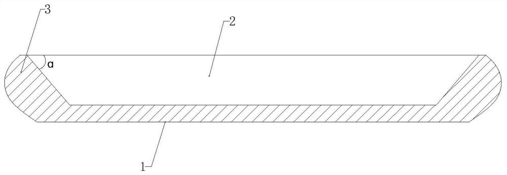
[0027] see Figure 1 to Figure 2 A wafer for preparing semiconductor devices according to a preferred embodiment of the present invention includes a wafer body 1, the back side of the wafer body is thinned to form a groove 2, and the wafer body is formed around the groove and positioned on the wafer The supporting ring 3 on the edge of the body is characterized in that: the side of the supporting ring, that is, the inner side of the groove, is an inclined plane.

[0028] The setting of the slope makes the slope of the inner surface of the support ring more gentle, so that the resist is not easy to remain between the support ring and the bottom wall of the groove during N-...


PUM

PropertyMeasurementUnit
widthaaaaaaaaaa
thicknessaaaaaaaaaa

Abstract

The invention relates to a wafer for preparing a semiconductor device. The wafer comprises a wafer body, wherein the back surface of the wafer body forms a groove through back surface thinning, the wafer body surrounds the groove to form a supporting ring positioned at the edge of the wafer body, and the side surface of the supporting ring, namely the inner side surface of the groove, is an inclined surface. According to the wafer for preparing the semiconductor device, photoresist is not easy to remain during back surface N-type exposure, so that the influence of the photoresist on equipmentduring annealing is avoided.

Description

technical field [0001] The invention relates to a wafer, in particular to a wafer used for preparing semiconductor devices. In addition, the present invention also designs a wafer backside thinning method. Background technique [0002] When preparing semiconductor devices such as RC-IGBT, it is necessary to perform N-type photolithography on the back of the wafer. Before lithography, the wafer must be thinned to a specified thickness (60um-130um), and the backside lithography equipment has higher requirements on the thickness of the wafer. At present, the backside lithography equipment cannot directly process thinner wafers Therefore, the current prior art uses the TAIKO process to grind the back of the wafer. [0003] The TAIKO process includes the following steps: attach a protective film (blue film or UV film) to the front of the wafer; grind the inside of the wafer (dry etching and wet etching) to a thin sheet (thickness less than 60-130um); remove the protective film;...

Claims


Application Information

Patent Timeline
Patent Type & Authority Applications(China)
IPC IPC(8): H01L29/06H01L21/304H01L21/306H01L21/308H01L21/331H01L29/739
CPCH01L29/0657H01L21/304H01L21/30604H01L21/308H01L29/7393H01L29/66325
Inventor 王海军阳平
Owner 上海擎茂微电子科技有限公司
Learn More