
Method for growing GaN film on graphene

A technology of graphene and graphene layer, which is applied in the direction of coating, gaseous chemical plating, metal material coating process, etc., can solve the problems such as the difficulty of GaN film formation, achieve low stress, promote lateral merger, and high crystal quality Effect

Pending Publication Date: 2020-12-08
JILIN UNIV
View PDF6 Cites 1 Cited by
  • Summary
  • Abstract
  • Description
  • Claims
  • Application Information

AI Technical Summary

Problems solved by technology

[0004] The purpose of the present invention is to solve the above-mentioned difficult problem of GaN film formation on graphene

Method used


Image

  • Method for growing GaN film on graphene
  • Method for growing GaN film on graphene
  • Method for growing GaN film on graphene

Examples


Embodiment 1

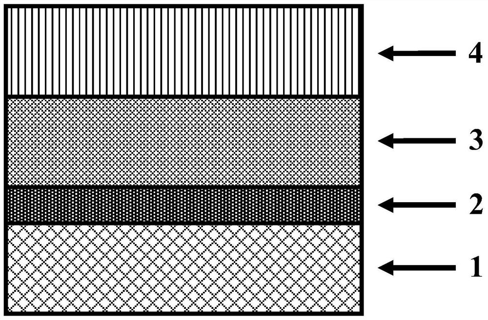
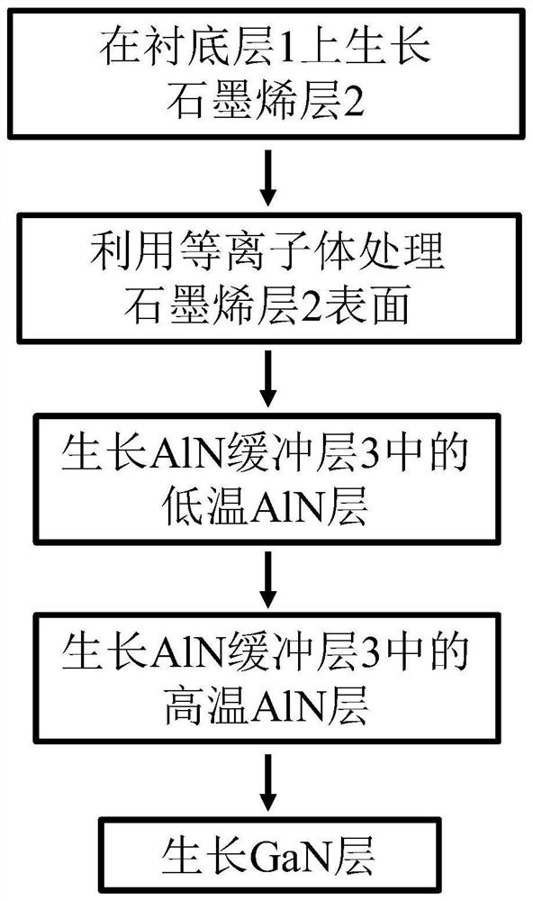
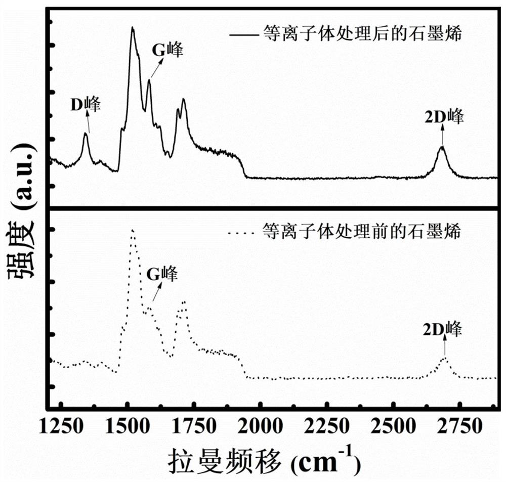
[0020] 1. A three-layer graphene layer 2 is grown on a SiC substrate 1 by a thermal decomposition SiC method. The SiC substrate 1 was annealed at 900° C. for 1 hour in an argon atmosphere, and the annealing pressure was 400 mbar. Then, continue heating to 1600° C. in an argon atmosphere at 800 mbar for 3 hours to realize the growth of three graphene layers 2 on the surface of the SiC substrate 1 . Then, the surface of the graphene layer is treated with plasma surface pretreatment technology, the working gas of plasma treatment is nitrogen, the temperature is room temperature, the power is 50W, and the treatment time is 30s. Afterwards, the MOCVD method is used to sequentially prepare an AlN buffer layer 3 (thickness 200nm) on the graphene layer 2 prepared on the SiC substrate 1, wherein the low-temperature AlN layer with a thickness of 40nm is first epitaxy, and then the remaining 160nm-thick high-temperature AlN layer is epitaxially increased in temperature. layer) and GaN l...


PUM

PropertyMeasurementUnit
thicknessaaaaaaaaaa
thicknessaaaaaaaaaa
thicknessaaaaaaaaaa

Abstract

The invention discloses a method for growing a GaN film on graphene, and belongs to the technical field of semiconductors. The method comprises the following steps: firstly, growing a graphene layer on a substrate layer, and then pretreating the surface of the grown graphene layer by utilizing plasma; then sequentially growing an AlN buffer layer and a GaN layer on the graphene layer in an epitaxial mode through an MOCVD method, wherein growth sources are trimethyl aluminum, trimethyl gallium and high-purity ammonia gas, the growth temperature ranges from 700 DEG C to 1300 DEG C, and the growth pressure intensity ranges from 50 mbar to 400 mbar; and growing on the graphene to obtain the GaN film. The AlN buffer layer is prepared by adopting a two-step temperature growth method, that is, alow-temperature AlN layer is extended outside the graphene layer at a low temperature(700-900 DEG C), and then a high-temperature AlN layer is extended continuously by raising the temperature(1000-1300 DEG C). According to the method disclosed by the invention, high-density AlN nucleation islands can be obtained on the graphene, and the transverse combination of the high-density AlN nucleation islands can be promoted, so that enough nucleation sites can be provided for the subsequent growth of GaN, and the epitaxial growth of the GaN film is realized.

Description

technical field [0001] The invention belongs to the technical field of semiconductors, and in particular relates to a method for growing a GaN thin film on graphene. Background technique [0002] The third-generation semiconductor materials represented by GaN have important application value in the fields of lighting, display, energy communication, national defense and military industry, and have been listed as "strategic advanced electronic materials" by my country. Currently, single-crystal GaN self-supporting substrates are expensive, and the epitaxial growth of GaN-based device structures is mainly based on heterogeneous substrates, and there are inevitably lattice mismatches and thermal problems between epitaxial GaN materials and substrates in heteroepitaxy. The mismatch causes a large number of point defects, line defects and residual stress in GaN materials and devices, which seriously hinders the improvement of the performance of GaN-based devices. [0003] The van...

Claims


Application Information

Patent Timeline
Patent Type & Authority Applications(China)
IPC IPC(8): H01L21/205C23C16/02C23C16/30
CPCH01L21/02458H01L21/0254H01L21/0262C23C16/0272C23C16/303
Inventor 张源涛余烨邓高强张宝林
Owner JILIN UNIV
Learn More