Mask plate of flash memory device and manufacturing method

A technology of flash memory device and manufacturing method, which is applied in the direction of electric solid-state devices, semiconductor devices, photoplate-making process of pattern surface, etc., can solve problems such as groove defects, achieve the effects of improving performance, increasing selection ratio, and avoiding defects

Pending Publication Date: 2020-12-11
SHANGHAI HUAHONG GRACE SEMICON MFG CORP
View PDF0 Cites 3 Cited by
  • Summary
  • Abstract
  • Description
  • Claims
  • Application Information

AI Technical Summary

Problems solved by technology

[0004] The object of the present invention is to provide a mask plate and a manufacturing method of a flash memory device, so as to solve the defect problem caused by the groove at the junction of the peripheral area and the storage area

Method used


Image

  • Mask plate of flash memory device and manufacturing method
  • Mask plate of flash memory device and manufacturing method
  • Mask plate of flash memory device and manufacturing method

Examples


Embodiment Construction

[0042] The mask plate and manufacturing method of the flash memory device proposed by the present invention will be further described in detail below in conjunction with the drawings and specific embodiments. The advantages and features of the present invention will become clearer from the following description. It should be noted that all the drawings are in a very simplified form and use imprecise scales, and are only used to facilitate and clearly assist the purpose of illustrating the embodiments of the present invention.

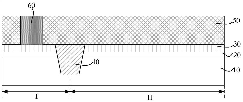
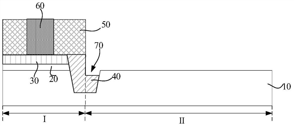
[0043]The inventors have found through research that the reason why the deep groove is formed at the junction of the peripheral area and the storage area in the prior art is that when forming a shallow trench isolation structure to define an active area, usually between the storage area and the peripheral area A shallow trench isolation structure is formed, that is, a shallow trench isolation structure is formed at the junction of the storage area and t...


PUM


Abstract

The invention provides a mask plate of a flash memory device and a manufacturing method, the mask plate of the flash memory device comprises an active area mask plate and a floating gate mask plate, the active area mask plate comprises a storage mask plate area and a peripheral mask plate area, a first active area pattern is arranged at the junction of the storage mask plate area and the peripheral mask plate area. According to the manufacturing method of the flash memory device, a first active area can be defined at the junction of a storage area and a peripheral area through an active area mask plate, and when a dielectric layer, a control gate layer, a floating gate layer and a floating gate oxide layer of the peripheral region are etched, due to the fact that the first active area is defined at the junction of the storage area and the peripheral area, in the etching process, if over-etching is generated, the over-etched etching object is the semiconductor substrate of the first active area, and compared with the prior art, the etching selection ratio can be improved, so that defects are avoided, and the performance of the flash memory device is further improved.

Description

technical field [0001] The invention relates to the field of semiconductor integrated circuit manufacturing, in particular to a mask plate of a flash memory device and a manufacturing method. Background technique [0002] At present, Flash memory, also known as flash memory, has become the mainstream of non-volatile memory. Its storage unit is based on the traditional MOS transistor structure, adding a floating gate (Floating Gate, FG) and a layer of Tunnel oxide (Tunnel Oxide), the current flash memory devices also prepare isolation regions by shallow trench isolation technology (STI, Shallow Trench Isolation). [0003] Such as figure 1 As shown in , it is a schematic diagram of the structure formed by the manufacturing method of the flash memory device in the prior art. A typical manufacturing method of a flash memory device in the prior art generally includes: a first step, providing a semiconductor substrate 10, sequentially forming a floating gate oxide layer 20 and a...

Claims


Application Information

Patent Timeline
Patent Type & Authority Applications(China)
IPC IPC(8): H01L27/11521H01L27/11531H01L27/11548G03F1/88
CPCG03F1/88H10B41/42H10B41/50H10B41/30
Inventor 陈宏
Owner SHANGHAI HUAHONG GRACE SEMICON MFG CORP
Why Eureka
Try Eureka