Gallium nitride enhanced HEMT device and preparation method thereof

An enhancement-mode, gallium nitride technology, applied in semiconductor/solid-state device manufacturing, semiconductor devices, electrical components, etc., can solve problems such as the inability to guarantee the reliability and stability of enhancement-mode HEMT devices, and reduce the surface state of high-concentration impurities. , reduce defects, improve the effect of on/off current ratio

Pending Publication Date: 2020-12-15
深圳市红与蓝企业管理中心(有限合伙)
View PDF5 Cites 7 Cited by
  • Summary
  • Abstract
  • Description
  • Claims
  • Application Information

AI Technical Summary

Problems solved by technology

[0004] Therefore, the technical problem to be solved by the present invention is to overcome the defect that the preparation method of the enhanced HEMT device in the prior art cannot guarantee the reliability and stability of the enhanced HEMT device, thereby providing a gallium nitride enhanced HEMT device and its preparation method

Method used


Image

  • Gallium nitride enhanced HEMT device and preparation method thereof
  • Gallium nitride enhanced HEMT device and preparation method thereof
  • Gallium nitride enhanced HEMT device and preparation method thereof

Examples


Embodiment 1

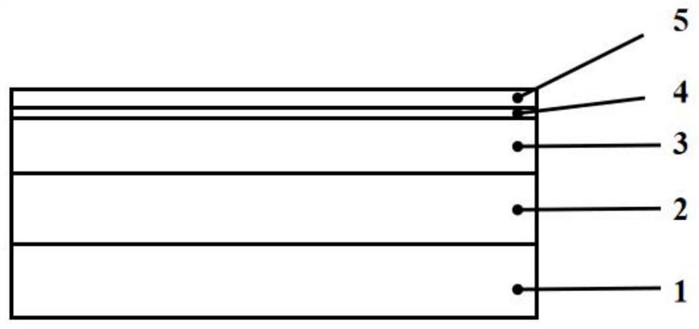
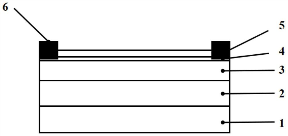
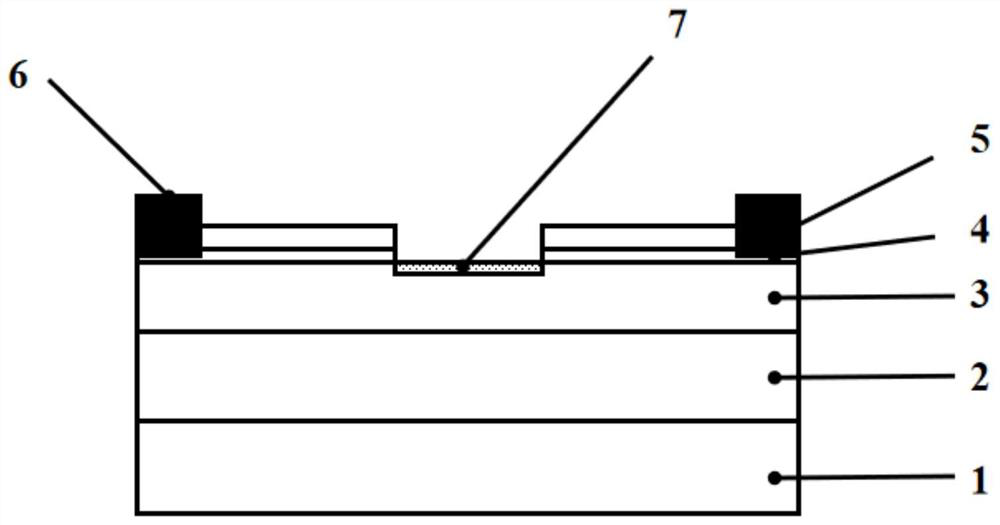
[0058] This embodiment provides a preparation method of a gallium nitride enhanced HEMT device, the structure of the device is as follows Figure 1-4 Shown, its preparation method comprises the following steps:

[0059] (1) Prepare a double-sided polished sapphire substrate.

[0060] (2) Use metal organic chemical vapor deposition (MOCVD) to grow on a sapphire substrate, 10 μm of non-doped GaN as a buffer layer; grow 50 μm of n-type GaN as a GaN layer, and the carrier concentration is about 8x10 16 cm -3 , trimethylhydrogensilane is used as the Si raw material for the n-type dopant (donor).

[0061] (3) On this basis, epitaxially grow AlGaN material as a heterogeneous barrier layer, wherein the Al composition is greater than 0 and less than 0.5, in this embodiment it is 0.2, and the thickness is 50nm; if the Al composition is too high, it is easy to produce Cracks, if the thickness is too low, are not enough to form a two-dimensional electron gas at the GaN material interfa...

Embodiment 2

[0068] This embodiment provides a preparation method of a gallium nitride enhanced HEMT device, the structure of the device is as follows Figure 1-4 Shown, its preparation method comprises the following steps:

[0069] (1) Prepare a double-sided polished GaN substrate.

[0070] (2) Use metal organic chemical vapor deposition (MOCVD) to grow on the GaN substrate, 12 μm of undoped GaN as a buffer layer; grow 60 μm of n-type GaN as the GaN layer, and the carrier concentration is about 8x10 16 cm -3 , trimethylhydrogensilane is used as the Si raw material for the n-type dopant (donor).

[0071] (3) On this basis, epitaxially grow AlGaN material as a heterogeneous barrier layer, wherein the Al composition is greater than 0 and less than 0.5, in this embodiment it is 0.3, and the thickness is 50nm; if the Al composition is too high, it is easy to produce Cracks, if the thickness is too low, are not enough to form a two-dimensional electron gas at the GaN material interface.

[...

Embodiment 3

[0078] This embodiment provides a preparation method of a gallium nitride enhanced HEMT device, the structure of the device is as follows Figure 1-4 Shown, its preparation method comprises the following steps:

[0079] (1) Prepare a double-sided polished GaN substrate.

[0080] (2) Growth on GaN substrate by metal-metal organic chemical vapor deposition (MOCVD), 8 μm of non-doped GaN as a buffer layer; growth of 30 μm n-type GaN as GaN layer, carrier concentration is about 8x10 16 cm -3 , trimethylhydrogensilane is used as the Si raw material for the n-type dopant (donor).

[0081] (3) On this basis, epitaxially grow AlGaN material as a heterogeneous barrier layer, wherein the Al composition is greater than 0 and less than 0.5, in this embodiment it is 0.3, and the thickness is 50nm; if the Al composition is too high, it is easy to produce Cracks, if the thickness is too low, are not enough to form a two-dimensional electron gas at the GaN material interface.

[0082] (4)...


PUM

PropertyMeasurementUnit
thicknessaaaaaaaaaa
thicknessaaaaaaaaaa
thicknessaaaaaaaaaa

Abstract

The invention belongs to the technical field of semiconductor materials and particularly relates to a gallium nitride enhanced HEMT device and a preparation method thereof. According to the method, ICP (Inductively Coupled Plasma) is adopted to optimize a gallium nitride conductive channel, oxygen plasma treatment is performed before an insulating dielectric layer is deposited, then in-situ annealing is performed, and a crystal GaON nano-phase is generated in a gate region to serve as an optimized channel layer. The method can effectively reduce the surface state of high-concentration impurities introduced by the inner wall of the groove due to the etching process and the morphology of the rough inner wall, improves the stability and reliability of the device, improves the breakdown voltage and on/off current ratio of the device, and further improves the working performance of the device.

Description

technical field [0001] The invention belongs to the technical field of semiconductor materials, and in particular relates to a gallium nitride enhanced HEMT device and a preparation method thereof. Background technique [0002] High electron mobility transistors (HEMTs) based on AlGaN / GaN heterojunctions have unique advantages such as low on-resistance, high breakdown voltage, and high switching frequency, so they can be used as core devices in various power conversion systems. There are important application prospects in reducing consumption, so it has received great attention from academia and industry. However, since the depletion-mode HEMT device is a normally-on device, a large amount of additional energy will be lost when the depletion-mode HEMT device is used for operation. The enhanced HEMT device does not have the above problems. Conventional enhanced HEMT devices are based on depletion-type HEMT devices, which deplete the two-dimensional electron gas under the ga...

Claims


Application Information

Patent Timeline
Patent Type & Authority Applications(China)
IPC IPC(8): H01L21/34H01L21/465H01L21/477H01L29/06H01L29/10H01L29/24H01L29/778B82Y30/00
CPCH01L29/66969H01L29/0665H01L29/1033H01L29/7787H01L29/24H01L21/465H01L21/477B82Y30/00
Inventor 刘新科林峰利键陈勇王磊黎晓华贺威俞文杰吕有明韩舜曹培江柳文军曾玉祥朱德亮
Owner 深圳市红与蓝企业管理中心(有限合伙)
Why Eureka
Try Eureka