An aromatic amine compound, an electronic component and an electronic device using the same
A compound, aromatic amine technology, applied in electrical components, silicon organic compounds, compounds of elements of Group 4/14 of the periodic table, etc. Effect of hole mobility, lowering of driving voltage, and lowering of crystallinity
- Summary
- Abstract
- Description
- Claims
- Application Information
AI Technical Summary
Problems solved by technology
Method used
Image
Examples
Embodiment 1
[0288] The anode was prepared by the following process: the thickness of ITO was The TOP substrate (manufactured by Corning) was cut into a size of 40mm (length) × 40mm (width) × 0.7mm (thickness), and it was prepared into an experimental substrate with a cathode bonding area, an anode and an insulating layer pattern using a photolithography process , using UV-ozone and O 2 :N 2 Plasma surface treatment was performed to increase the work function of the anode (experimental substrate) and to remove scum.
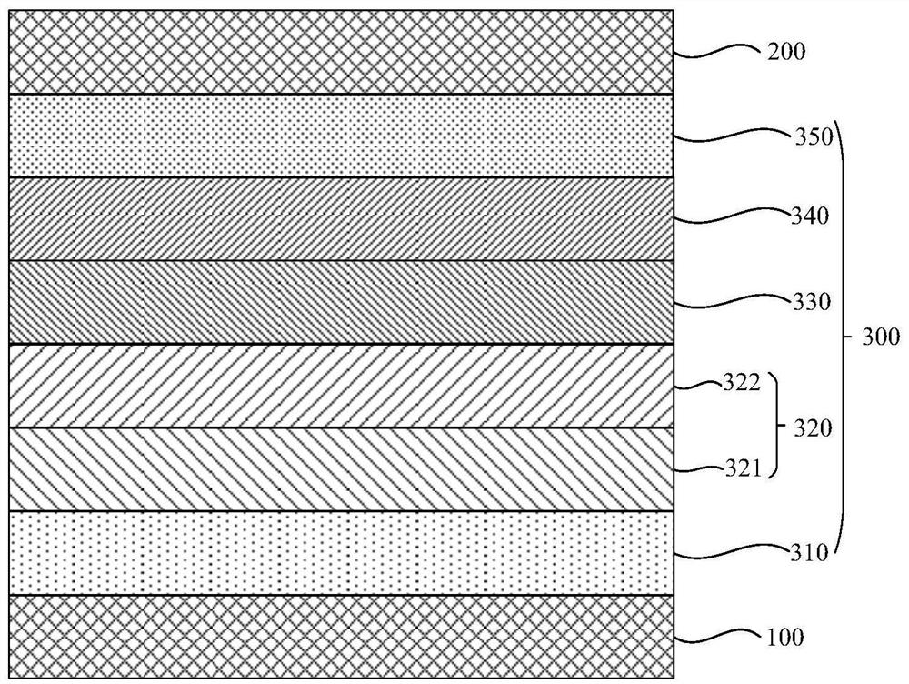
[0289] Vacuum-deposit m-MTDATA (4,4',4"-tris(N-3-methylphenyl-N-phenylamino)triphenylamine) on the experimental substrate (anode) to form a thickness of The hole injection layer (HIL), and the compound 22 is vacuum evaporated on the hole injection layer to form a thickness of The first hole transport layer (HTL1).
[0290] Then evaporate EB-1 on the first hole transport layer to form a thickness of The second hole transport layer (HTL2).
[0291] Then α, β-ADN is us...
Embodiment 2~7
[0297] An organic electroluminescence device was fabricated by the same method as in Example 1, except that the compounds shown in Table 7 were each used in forming the first hole transport layer (HTL1). Device performance is listed in Table 7.
Embodiment 8
[0310] The anode was prepared by the following process: the thickness of ITO was The ITO substrate (manufactured by Corning) was cut into a size of 40mm (length) × 40mm (width) × 0.7mm (thickness), and it was prepared into an experimental substrate with cathode, anode and insulating layer patterns by using a photolithography process. Ozone and O 2 :N 2 Plasma surface treatment was performed to increase the work function of the anode (experimental substrate) and to remove scum.
[0311] HAT-CN was vacuum evaporated on the experimental substrate (anode) to form a thickness of The hole injection layer (HIL), and a layer of NPB is evaporated on the hole injection layer to form a thickness of The first hole transport layer (HTL1).
[0312] Then vacuum evaporate compound 113 on the first hole transport layer to form a thickness of The second hole transport layer (HTL2).
[0313] Then vapor-deposit 4,4'-N,N'-dicarbazole-biphenyl (referred to as "CBP") on the second hole tra...
PUM
 Abstract
Description
Claims
Application Information


