GaN film and preparation method thereof

A thin film and thin film layer technology, applied in the field of GaN thin film and its preparation, can solve problems such as Ga-Si melting back etching, achieve the effect of avoiding melting back etching, avoiding quantum confinement Stark effect, and improving quality

Pending Publication Date: 2020-12-25
LANZHOU UNIVERSITY
View PDF6 Cites 3 Cited by
  • Summary
  • Abstract
  • Description
  • Claims
  • Application Information

AI Technical Summary

Problems solved by technology

The buffer layer Si in the GaN film of the present invention 3 N 4 The layer is an ordered hexagonal close-packed structure, which can not only solve the problems caused by lattice mismatch and thermal mismatch, but also avoid Ga-Si remelting and etching, as well as relaxation and compensation for subsequent GaN growth accumulation. residual stress

Method used


Image

  • GaN film and preparation method thereof
  • GaN film and preparation method thereof
  • GaN film and preparation method thereof

Examples


Embodiment 1

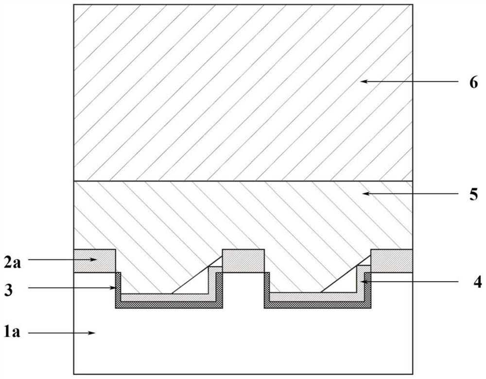
[0035] Such as figure 1 As shown, a GaN thin film, including Si substrate 1a and SiO patterned on Si substrate 1a 2 A mask layer 2a, the Si {111} crystal plane of the Si substrate 1a has Si 3 N 4 buffer layer 3, the SiO 2 Mask layer 2a and Si not involved in GaN growth 3 N 4 Buffer layer 3 with sputtered SiO 2 Film 4; the Si involved in GaN growth 3 N 4 There is a GaN insertion layer 5 on the buffer layer 3 , and a GaN thin film layer 6 is grown on the GaN insertion layer 5 . The SiO 2 The mask layer 2 a has a thickness of 50-100 nm and is a strip mask layer, wherein the width of the strip mask layer is 1-3 μm, and the distance between each strip mask layer is 3-10 μm. The Si that does not participate in GaN growth 3 N 4 The buffer layer 3 has a thickness of 20-100nm, the GaN insertion layer 5 has a thickness of 200-400nm, and the sputtered SiO 2 The thickness of the film 4 is 40-60nm, and the thickness of the GaN thin film layer 6 is 1000-2000nm.

[0036] Wherein...

Embodiment 2

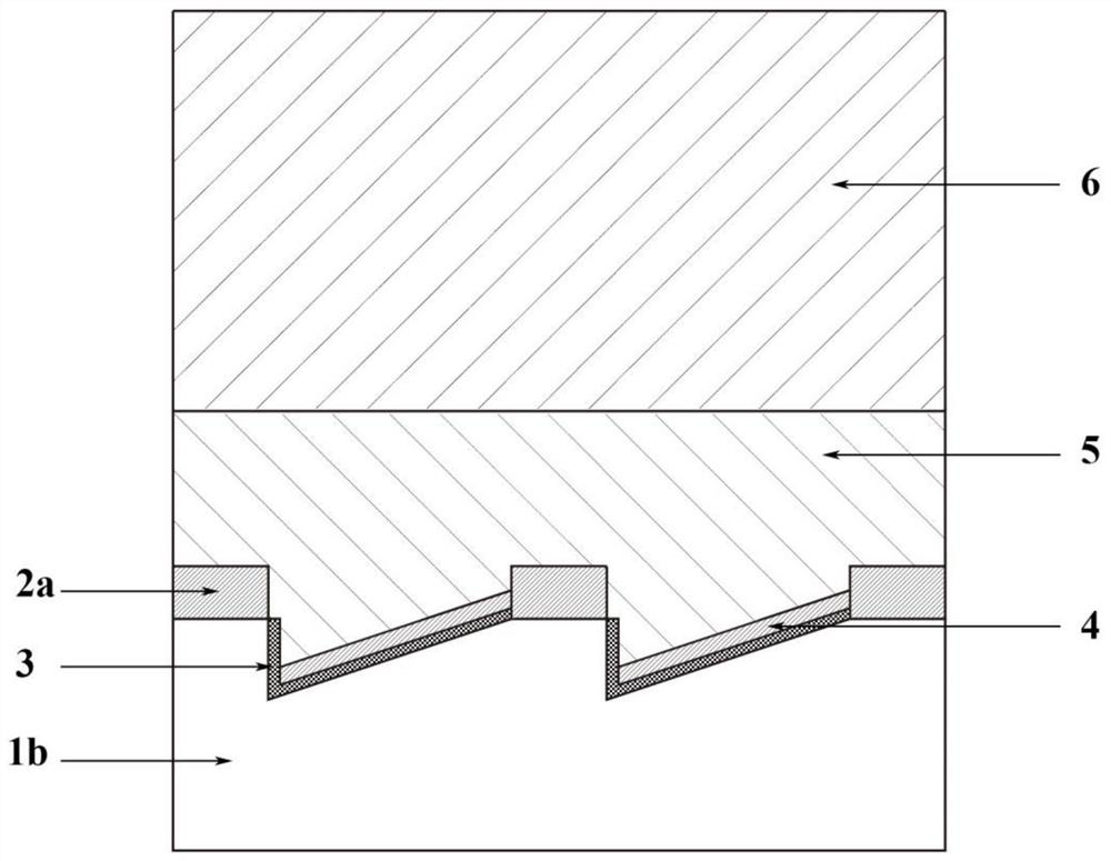
[0041] Such as figure 2 Shown: the difference between this embodiment 2 and embodiment 1 is only that the Si substrate 1b of the GaN thin film has a (112) crystal orientation, and the crystal plane of the Si substrate 1b includes a (112) crystal plane, so The etched Si{111} includes (-1-11) crystal plane and (111) crystal plane; used for growing Si 3 N 4 The Si{111} crystal plane of the buffer layer 3 is the (-1-11) crystal plane; the crystal plane on which the GaN thin film layer 6 is grown is the (1-100) crystal plane.

Embodiment 3

[0043] A method for preparing a GaN film, specifically comprising the steps of:

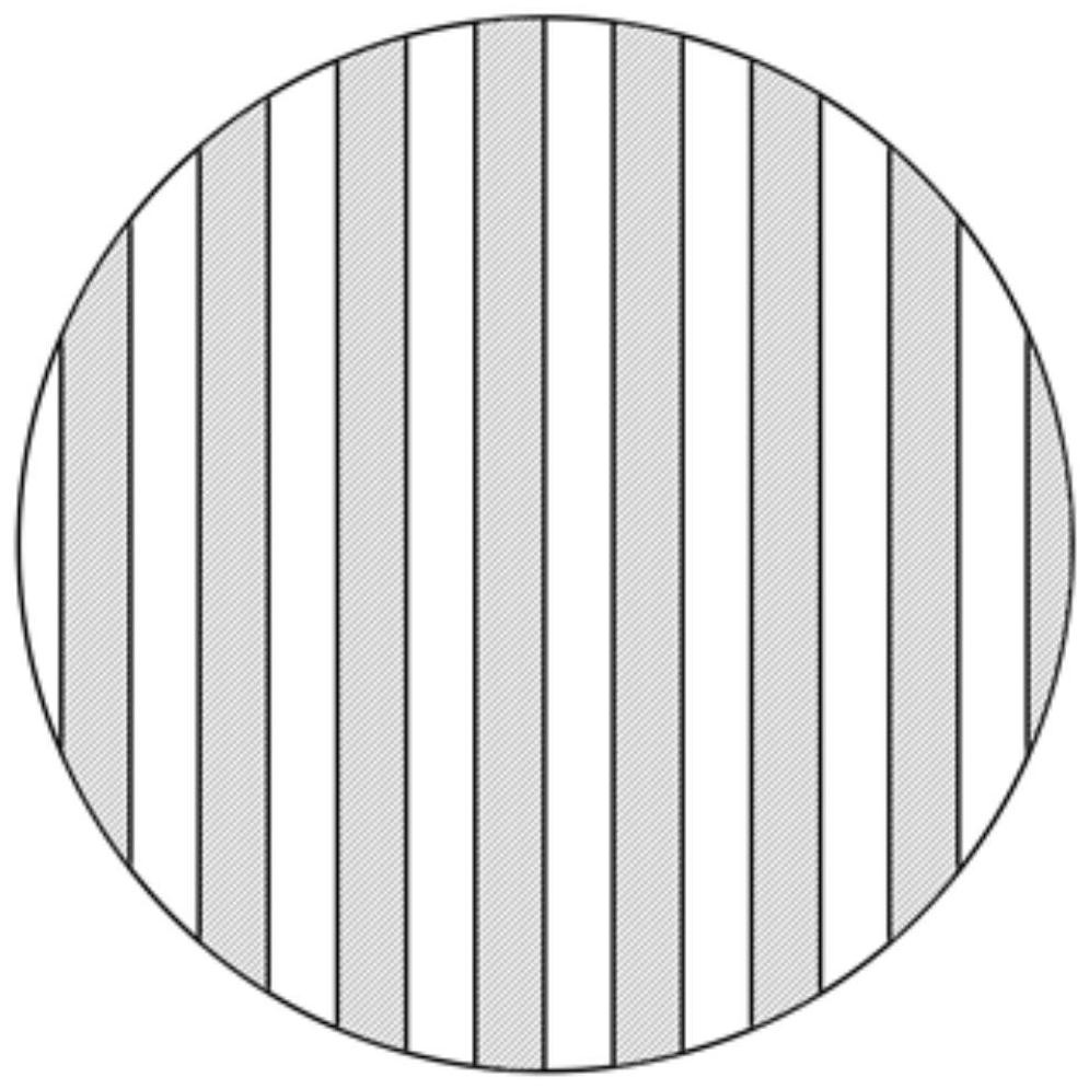
[0044] Step 1), grow a layer of 50-100nm SiO on the substrate 1a of Si(110) by plasma-enhanced chemical vapor deposition (PECVD) 2 Film 2, photoresist pattern transferred to SiO by photolithography process 2 film 2, and then patterned SiO was fabricated by inductively coupled plasma (ICP) etching 2 mask layer 2a, the SiO 2 The mask layer 2a is a strip mask layer, wherein the width of the strip mask layer is 1-3 μm, and the distance between each strip mask layer is 3-10 μm, such as image 3 shown; then, by wet etching, use a KOH solution with a mass concentration of 20%-40% at a temperature of 30°C-40°C for 10-20min, etch to form a groove on the surface of the Si substrate 1a, The sides of the groove are Si {111} crystal planes, including (-111) crystal planes and (1-1-1) crystal planes, such as Figure 5 shown;

[0045] Step 2), nitriding the Si {111} crystal plane etched in step 1), that is...


PUM

PropertyMeasurementUnit
thicknessaaaaaaaaaa
thicknessaaaaaaaaaa
thicknessaaaaaaaaaa

Abstract

The invention relates to a GaN film and a preparation method thereof. The GaN film comprises a Si substrate and a patterned SiO2 mask layer located on the Si substrate, a Si3N4 buffer layer is arranged on the Si {111} crystal face of the Si substrate, and a sputtered SiO2 film is arranged on the SiO2 mask layer and the Si3N4 buffer layer which does not participate in GaN growth. A GaN insertion layer is arranged on the Si3N4 buffer layer participating in GaN growth, and a GaN film layer grows on the GaN insertion layer. The GaN film provided by the invention is prepared by a method of epitaxially growing a non-polar GaN film on the Si patterned substrate, is low in cost and excellent in performance, and can be widely applied to manufacturing of devices.

Description

technical field [0001] The invention relates to the field of semiconductors, in particular to a GaN thin film epitaxially growing non-polar GaN on a Si pattern substrate and a preparation method thereof. Background technique [0002] GaN is a wide-bandgap semiconductor with a direct bandgap. Due to its excellent properties such as high thermal conductivity, high-intensity field drift speed and high breakdown voltage, it has attracted widespread attention and has been used in many optoelectronic and high-power electronic devices. . At present, in terms of chargers, GaN materials can be made into small-sized, high-power fast chargers, which have great prospects in the fast charging market; and lighting devices such as LEDs made of GaN materials have been commercialized. In addition, in the 5G era, GaN will also be used in base station power amplifiers due to its small size, high efficiency and high power density. . [0003] At this stage, sapphire (Al 2 o 3 ) and silicon ...

Claims


Application Information

Patent Timeline
Patent Type & Authority Applications(China)
IPC IPC(8): H01L33/12H01L33/32H01L21/02H01L33/00C23C14/10C23C14/34C23C16/30C23C16/40C23C16/50C23C28/04
CPCH01L33/12H01L33/32H01L33/007H01L21/02381H01L21/02433H01L21/02488H01L21/0254H01L21/0262C23C16/50C23C16/402C23C14/34C23C14/10C23C28/04C23C16/303
Inventor 赵桂娟邢树安刘贵鹏汤金金
Owner LANZHOU UNIVERSITY
Why Eureka
Try Eureka