Connecting method of ZrB2-based ceramic
A connection method and ceramic technology, applied in the connection field of ZrB2-based ceramics, can solve the problems of uneven distribution of elements in the connection area, reduced grain growth of the ceramic matrix, poor structural integrity of the joint, etc. The effect of grain growth and rapid temperature rise
- Summary
- Abstract
- Description
- Claims
- Application Information
AI Technical Summary
Problems solved by technology
Method used
Image
Examples
Embodiment 1
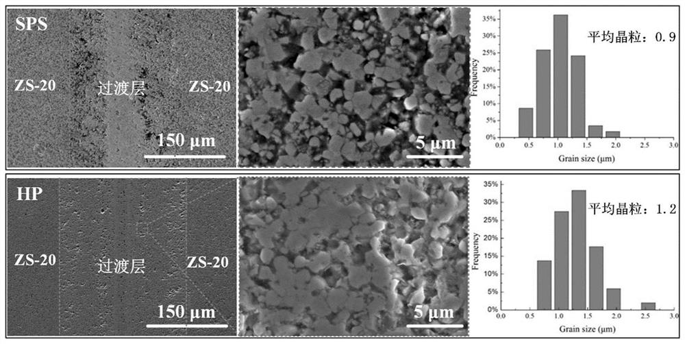
[0028] Ni powder is used as brazing filler, and the thickness of the raw material is 50 μm, because of its ZrB 2 The diameter of the base ceramic matrix is 20mm, so the Ni powder is 15.7mg, and the powder particle size is 500nm; the Ni powder is dried in a vacuum oven for 10h; the ZrB is connected by the spark plasma sintering method. 2 -SiC ceramics, heated up to 1200°C at 50°C / min in a vacuum atmosphere, held for 30 minutes, cooled to 600°C at 25°C / min, and then cooled to room temperature with the furnace, and the pressure was set to 10MPa during the whole process. Under the same process parameters, ZrB was connected with SPS by HP method 2 base ceramics. The microstructure of the connected samples is as follows: figure 1 As shown, it can be clearly found that there are no obvious defects in the microscopic morphology of the joints obtained by the HP method and the SPS method, but on the joints, the grains of the joints connected by the SPS method are smaller, and it can...
Embodiment 2
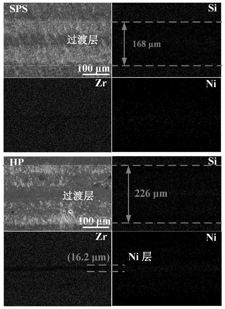
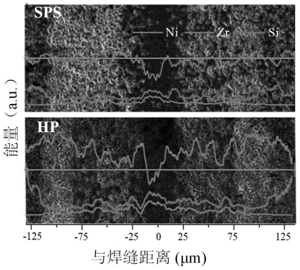
[0030] Ni powder is used as brazing filler, the raw material thickness is 50μm, ZrB 2 The diameter of the base ceramic substrate is 20mm, the Ni powder is 15.7mg, and the Ni powder particle size is 500nm; the Ni powder is dried in a vacuum oven for 12h; the ZrB is connected by the spark plasma sintering method 2 The base ceramics were heated up to 1200°C at 50°C / min in a vacuum atmosphere, held for 25 minutes, cooled to 600°C at 25°C / min, and then cooled to room temperature with the furnace, and the pressure was set to 10MPa during the whole process. The element distribution of the connected sample is as follows figure 2 , as shown in 3, it can be clearly found that the element distribution of the joints obtained by the HP method and the SPS method is relatively uniform. However, in the joints connected by the HP method, the Ni element has obvious weak areas, from Figure three It can be seen that the elements of the joints connected by SPS are more uniform than those conne...
Embodiment 3
[0032] Ni powder is used as brazing filler, and the thickness of the raw material is 50 μm, because of its ZrB 2 The diameter of the base ceramic matrix is 20mm, so the Ni powder is 14.13mg, and the powder particle size is 500nm; the Ni powder is dried in a vacuum oven for 10h; the ZrB is connected by the spark plasma sintering method. 2 -SiC ceramics, heated up to 1200°C at 50°C / min in a vacuum atmosphere, held for 30 minutes, cooled to 600°C at 25°C / min, and then cooled to room temperature with the furnace, and the pressure was set to 10MPa during the whole process.
[0033] Example 3
[0034] Ni powder is used as brazing filler, and the thickness of the raw material is 45 μm, because of its ZrB 2 The diameter of the base ceramic matrix is 20mm, so the Ni powder is 14.13mg, and the powder particle size is 500nm; the Ni powder is dried in a vacuum oven for 10h; the ZrB is connected by the spark plasma sintering method. 2-SiC ceramics, heated up to 1200°C at 50°C / min in ...
PUM
| Property | Measurement | Unit |
|---|---|---|
| thickness | aaaaa | aaaaa |
| diameter | aaaaa | aaaaa |
| particle diameter | aaaaa | aaaaa |
Abstract
Description
Claims
Application Information


