Preparation method of a light-modulating terahertz absorbing device with an all-carbon structure

A carbon structure, terahertz technology, applied in optical components, instruments, optics, etc., can solve the problems of single-layer graphene being difficult to process, low terahertz reflection intensity, and inability to carry out optical signals, so as to avoid low sublimation growth density, High terahertz response intensity and the effect of enhancing terahertz signals

Active Publication Date: 2022-05-17
HANGZHOU GAOXI TECH CO LTD
View PDF2 Cites 0 Cited by
  • Summary
  • Abstract
  • Description
  • Claims
  • Application Information

AI Technical Summary

Problems solved by technology

In the field of terahertz molecular detection, conventionally used materials are metals and semimetals, which have two serious problems: first, they have poor molecular affinity, especially with molecules containing conjugated structures; second, they cannot carry out optical signals. Modulation, unable to respond to changes in the external optical environment
However, single-layer graphene is not easy to process and is easily damaged, resulting in a rapid decrease in conductivity and poor processing continuity. At the same time, the terahertz reflection intensity is too low, so it is not suitable for making terahertz absorbers.

Method used


Image

  • Preparation method of a light-modulating terahertz absorbing device with an all-carbon structure
  • Preparation method of a light-modulating terahertz absorbing device with an all-carbon structure
  • Preparation method of a light-modulating terahertz absorbing device with an all-carbon structure

Examples


Embodiment 1

[0040] (1) Assemble a graphene oxide solution (0.5ug / mL) on an anodized aluminum substrate by spin coating to form a graphene oxide film with a thickness of 40 atomic layers, and chemically reduce the graphene oxide film. The reduction condition is HI as the reducing agent, Treat at 60°C for 4h.

[0041] (2) FeCl 3 (100°C) is uniformly vapor-deposited on the surface of the reduced nano-film, cooled, solidified and shrunk to obtain an exfoliated graphene nano-film.

[0042] (3) With a heating rate of 10°C / min, the graphene oxide film was heated up to 1200°C by electric heating, and kept for 4h to obtain a graphene film layer with high defects and high terahertz transmission, with a defect content of 30%; the graphite oxide The temperature of the olefin film was raised to 2300 °C and kept for 2 h to reduce the defects of the graphene oxide film to 0.2%.

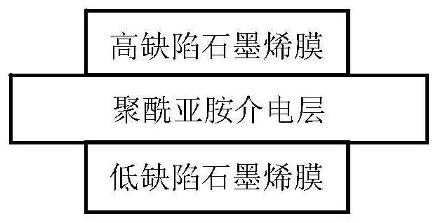
[0043] (4) The obtained high-defect graphene film and low-defect graphene film are attached to the front and back of the po...

Embodiment 2

[0045] (1) Assemble a graphene oxide solution (0.5ug / mL) on a glass fiber substrate to form a 60-atom-layer-thick graphene film by suction filtration, and then chemically reduce the nanofilm. The reduction condition is HI as the reducing agent, and 90 ° C for 2 hours .

[0046] (2) AlCl 3 (183°C) is uniformly vapor-deposited on the surface of the nano-film, cooled, solidified and shrunk to obtain an exfoliated graphene nano-film.

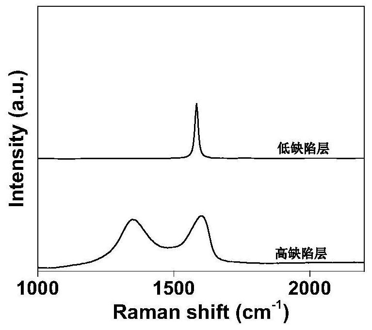
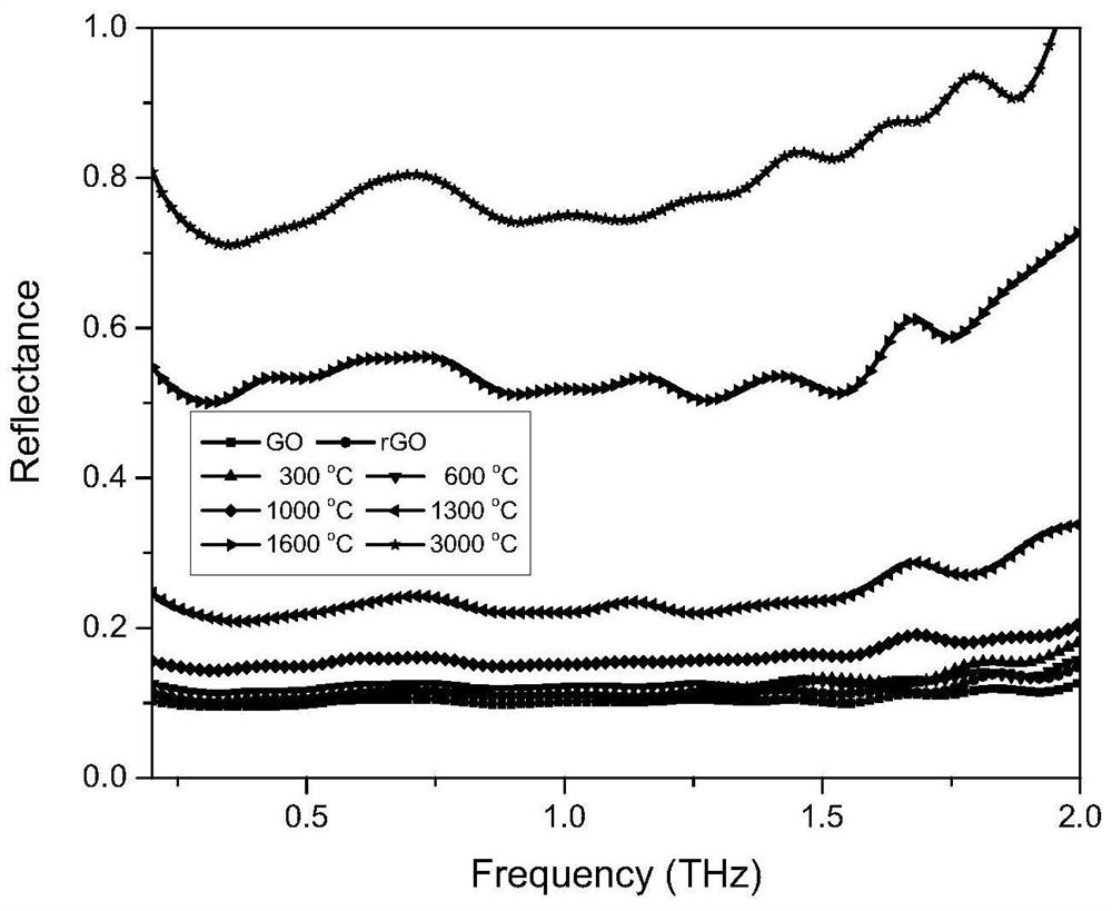
[0047] (3) With a heating rate below 20° C. / min, the graphene oxide film is heated by infrared radiation to 1300° C. and kept for 4 hours to obtain a graphene film layer with high defects and high terahertz transmission, and the defect content is 50% ( figure 1 , its SEM image is shown in Figure 6 Shown); graphene oxide film is heated up to 2000 ℃, and keeps 4h, to reduce the defect of graphene oxide film to below 0.3% ( figure 1 ). As the temperature increases, the graphene structure is gradually repaired, and the terahertz reflection of the g...

Embodiment 3

[0050] (1) Assemble graphene oxide (0.5ug / mL) on the mixed cellulose ester substrate by suction filtration to form a graphene film with a thickness of 180 atomic layers, and then chemically reduce the nanofilm.

[0051] (2) AlCl 3 (183°C) is evenly evaporated on the surface of the nanometer film, cooled and solidified to etch the substrate (mixed cellulose ester as the substrate), and the exfoliated graphene nanofilm is obtained.

[0052] (3) With a heating rate of 30°C / min, the graphene oxide film was heated to 1400°C by microwave heating, and kept for 2h to obtain a graphene film layer with high defects and high terahertz transmission, with a defect content of 20%; the graphite oxide The temperature of the olefin film was raised to 3000 °C and kept for 1 h to reduce the defects of the graphene oxide film to 0.3%.

[0053] (4) Attach the obtained high-defect graphene film and low-defect graphene film to the front and back of the polyimide film to form a flexible terahertz ab...


PUM


Abstract

The invention discloses a method for preparing a light-modulating terahertz absorbing device with an all-carbon structure. The method utilizes simple chemical assembly and reduction, and molecular crystal-assisted transfer to obtain independently supported graphene nanomaterials. The sintering temperature and time are regulated to obtain Defect-controllable graphene film structure. The film has good terahertz permeability or shielding property. The thin film polyimides with different structures are assembled layer by layer to form a sandwich structure, and placed under terahertz light. As the concentration of molecules added to the surface increases, the peak position of the terahertz transmission spectrum will change accordingly, so it can be prepared as The terahertz molecular detection device is used to detect molecular residues; at the same time, the double-layer graphene nano-film layer can be optically regulated and can be used to detect changes in optical intensity. In addition, using the combination of the two etching methods to increase the specific surface area in different scales, under the same dropwise addition of molecular content detection, it will have a greater change in the electrical properties of the material, and the change in the terahertz signal will be greater.

Description

technical field [0001] The invention relates to a preparation method of a light modulation terahertz absorbing device with an all-carbon structure. Background technique [0002] Terahertz molecular detection uses terahertz as the basic light source to detect the influence of molecules on the conductivity of terahertz metamaterials. Its advantage is that it can detect the concentration of drug molecules quickly, in batches, and in real time. In the field of terahertz molecular detection, conventionally used materials are metals and semimetals, which have two serious problems: first, they have poor molecular affinity, especially with molecules containing conjugated structures; second, they cannot carry out optical signals. Modulation, unable to respond to changes in the external optical environment. [0003] Recently, the rapid rise of single-layer graphene provides an alternative material for terahertz molecular detection, which has good phototunability, electrical modulati...

Claims


Application Information

Patent Timeline
Patent Type & Authority Patents(China)
IPC IPC(8): G02B5/00G02F1/17
CPCG02B5/003G02F1/17Y02P70/50
Inventor 彭蠡文章高超
Owner HANGZHOU GAOXI TECH CO LTD
Why Eureka
Try Eureka