Micro-channel inlet cover plate and preparation method and use method thereof
A technology of micro-channels and inlet caps, applied in chemical instruments and methods, laboratory containers, instruments, etc., can solve the problems of hose shedding and inability to achieve smaller sizes, and achieve high connection strength and bonding performance Good, guarantee the effect of consistency
- Summary
- Abstract
- Description
- Claims
- Application Information
AI Technical Summary
Problems solved by technology
Method used
Image

Examples
preparation example Construction
[0058] A preparation method of a microchannel inlet cover plate, such as Figure 5 shown, including the following steps:
[0059] Step 1. Photolithography: Spin-coat photoresist on the surface of the wafer, perform photolithography, and define the opening pattern and position of the top large hole 2, where the photoresist is used as an etching mask.
[0060] Step 2. Top etching: BOSCH process is used for plasma etching to etch the top large hole 2 .
[0061] After the large hole 2 on the top is etched, the wafer is immersed in an organic solvent to remove the photoresist on the top.
[0062] Step 3. Temporary Bonding: Use temporary bonding glue to temporarily bond the glass slide to the top of the wafer, then turn it upside down.
[0063] Step 4. Secondary photolithography: Spin-coat photoresist on the surface of the inverted wafer, perform photolithography, and define the opening pattern and position of the small holes 3 at the bottom; wherein the photoresist is used as an ...
Embodiment 1
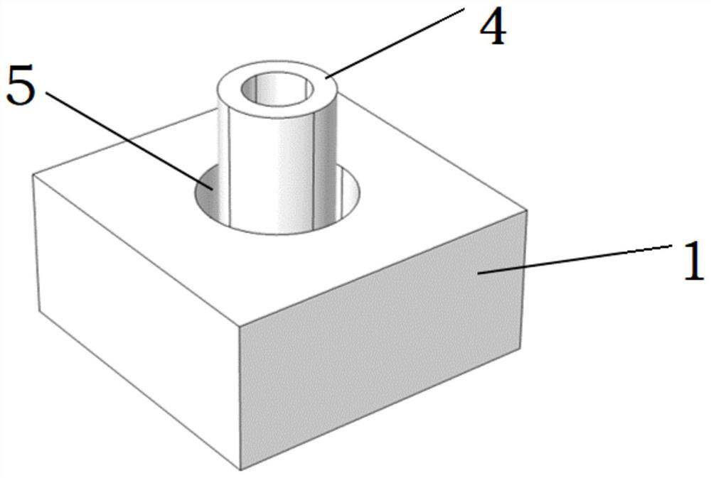
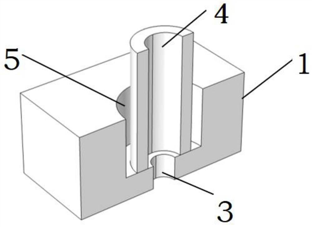
[0072] A microchannel inlet cover plate includes a cover plate unit 1 and a connecting pipe 4 . The cover unit 1 is a silicon cover, and the overall thickness of the cover unit 1 is 700um. The connecting pipe 4 is a stainless steel pipe, the inner diameter of the stainless steel pipe is 300um, the outer diameter is 500um, and the height is 15mm.
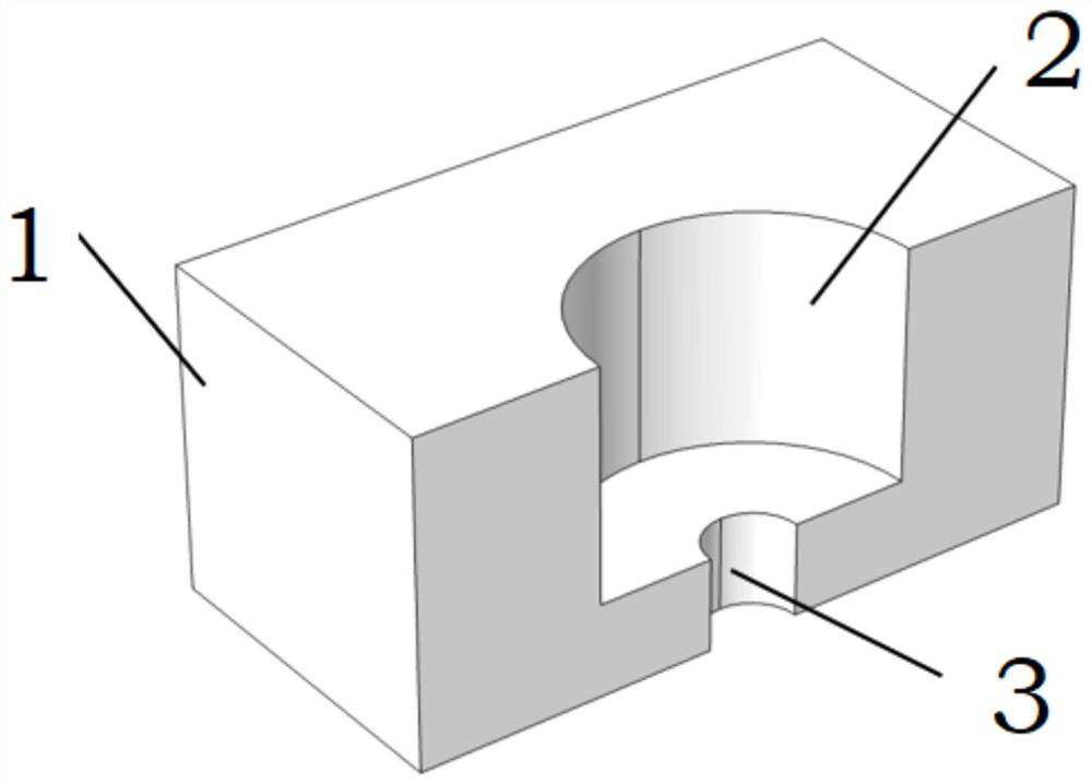
[0073] The cover plate unit 1 is provided with a stepped hole, and the stepped hole is composed of a top large hole 2 and a bottom small hole 3, and the top large hole 2 and the bottom small hole 3 are arranged coaxially. The depth of the large hole 2 at the top is 500um and the diameter is 600um, and the depth of the small hole 3 at the bottom is 200um and the diameter is 200um.
[0074] The connecting pipe 4 is arranged in the large hole 2 at the top of the cover unit 1 , and the bottom of the connecting pipe 4 is in contact with and fixed on the upper surface of the small hole 3 at the bottom.
Embodiment 2
[0076] A method for preparing a microchannel inlet cover plate, comprising the following steps:
[0077] A silicon wafer with a thickness of 700 um is used to prepare a silicon cover plate, and the connecting pipe 4 is a stainless steel pipe with an inner diameter of 0.3 mm and an outer diameter of 0.5 mm.
[0078] Step 1. Spin-coat photoresist with a thickness of 10um on the surface of the silicon wafer, perform photolithography, and open holes with an aperture of 600um;
[0079] Step 2. Use the deep silicon etching BOSCH process to perform plasma etching on the top of the silicon wafer, and the etching depth is about 500um;
[0080] Step 3. Use temporary bonding glue to temporarily bond the glass slide to the top of the silicon wafer, then turn it upside down;
[0081] Step 4. Spin-coat photoresist with a thickness of 10um on the surface of the inverted silicon wafer, and perform photolithography to define the opening pattern and position of the bottom small hole 3; wherein...
PUM
| Property | Measurement | Unit |
|---|---|---|
| Depth | aaaaa | aaaaa |
| Depth | aaaaa | aaaaa |
| Thickness | aaaaa | aaaaa |
Abstract
Description
Claims
Application Information
 - Generate Ideas
- Intellectual Property
- Life Sciences
- Materials
- Tech Scout
- Unparalleled Data Quality
- Higher Quality Content
- 60% Fewer Hallucinations
Browse by: Latest US Patents, China's latest patents, Technical Efficacy Thesaurus, Application Domain, Technology Topic, Popular Technical Reports.
© 2025 PatSnap. All rights reserved.Legal|Privacy policy|Modern Slavery Act Transparency Statement|Sitemap|About US| Contact US: help@patsnap.com