Self-assembled gap-adjustable gold nano-film preparation method
A gold nano and self-assembly technology, which is applied in the direction of nanotechnology, nanotechnology, nanotechnology, etc. for materials and surface science, can solve the problems of poor uniformity of nano-gold discs, difficult control of components, and impurity pollution, etc., to achieve Excellent optical and catalytic properties and biocompatibility, good market prospects, strong binding effect
- Summary
- Abstract
- Description
- Claims
- Application Information
AI Technical Summary
Problems solved by technology
Method used
Image
Examples
Embodiment 1
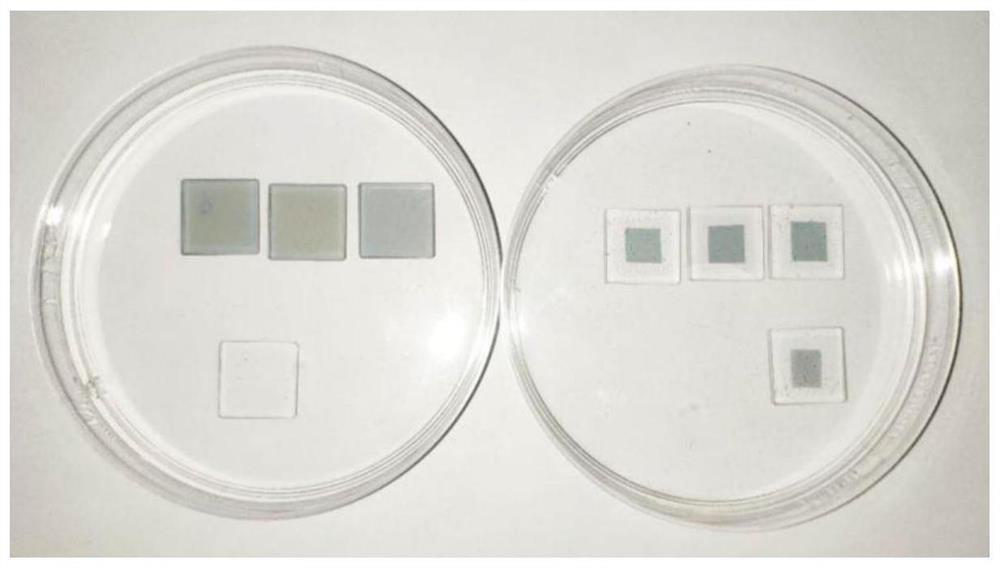
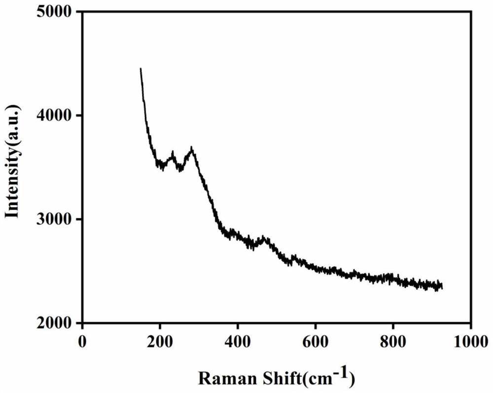
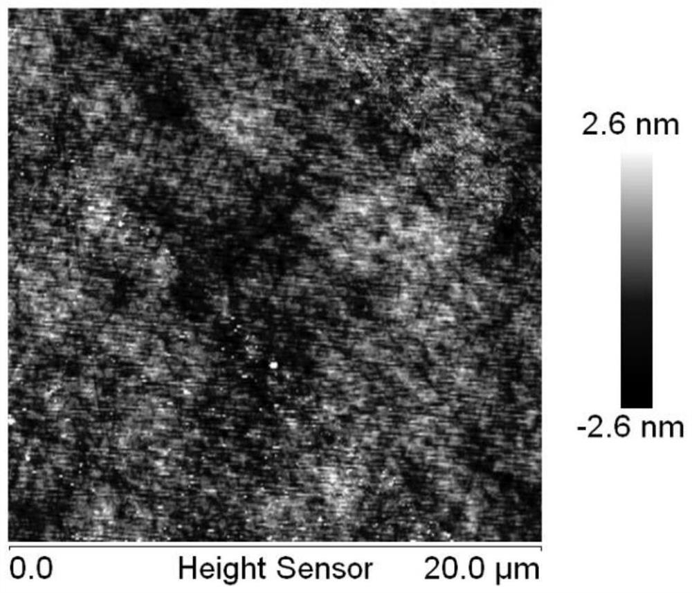
[0028] Example 1: Preparation process of self-assembled gold nanodisks with adjustable gap
[0029] a) Base cleaning
[0030] Choose a transparent siliceous quartz plate as the substrate and clean it. First put the base quartz plate into detergent / deionized water mixture, isopropanol, and acetone for ultrasonic cleaning for 5 minutes. Rinse with plasma water and dry with inert gas to ensure that the surface of the base quartz plate is clean and free of impurities. The power of ultrasonic cleaning is 150W, and the ultrasonic frequency is 40KHz.
[0031] b) Substrate pretreatment
[0032] Put the cleaned and dried base quartz plate into the plasma cleaning machine, with the side to be surface treated facing up, vacuumize for 2 minutes, the pressure in the chamber reaches 10Pa, the working power is 50W, and the cleaning frequency is 50Hz. The residual oxygen molecules are ionized into oxygen ions , the plasma surface was treated for 1 min, and the treated substrate was taken ou...
Embodiment 2
[0044] In this embodiment, the sputtering time of step c) is 20s, 30s, 40s, 50s, 60s, and other implementation conditions are the same as in Example 1, and the thicknesses of the corresponding self-assembled gold nanodiscs are 8.1nm, 11.8nm, and 17.0nm respectively. , 24.6nm, 35nm, the particle gap is 26-36nm, 19-25nm, 13-18nm, 8-12nm, 3-7nm, the thickness of the self-assembled nano gold disk and the particle gap are related to the sputtering time, the longer the sputtering time , the larger the thickness of the nano-gold film, the smaller the gap between the particles.
Embodiment 3
[0046] In this embodiment, step c) the distance between the gold target and the substrate quartz plate is 3cm, 4cm, 5cm, 6cm, 7cm, other implementation conditions are the same as in Example 1, and the thicknesses of the corresponding self-assembled nano-gold disks are 7.5nm, 6.8nm, respectively. nm, 5.6nm, 4.3nm, 2.7nm, particle gap respectively 28-30nm, 31-33nm, 34-37nm, 38-42nm, 42-47nm, self-assembled nano-gold disk thickness and particle gap with gold target and substrate quartz sheet There is a relationship between the distance between the gold target and the base quartz plate, the larger the distance between the gold target and the substrate quartz plate, the smaller the thickness of the nano-gold film, and the larger the gap between the particles.
PUM
| Property | Measurement | Unit |
|---|---|---|
| thickness | aaaaa | aaaaa |
| thickness | aaaaa | aaaaa |
Abstract
Description
Claims
Application Information
 - R&D
- Intellectual Property
- Life Sciences
- Materials
- Tech Scout
- Unparalleled Data Quality
- Higher Quality Content
- 60% Fewer Hallucinations
Browse by: Latest US Patents, China's latest patents, Technical Efficacy Thesaurus, Application Domain, Technology Topic, Popular Technical Reports.
© 2025 PatSnap. All rights reserved.Legal|Privacy policy|Modern Slavery Act Transparency Statement|Sitemap|About US| Contact US: help@patsnap.com


