Method for preparing graphene crystal film through electron beam scanning
An electron beam scanning and graphene technology, which is applied in crystal growth, chemical instruments and methods, single crystal growth, etc., can solve the problem that the efficiency of graphene crystal film is difficult to be greatly improved, the diameter of laser beam spot is small, and the quality of graphene crystal is easy to be affected. Eliminate the influence of gas impurities and other issues, and achieve the effects of high energy conversion efficiency, good quality, and simplified process
- Summary
- Abstract
- Description
- Claims
- Application Information
AI Technical Summary
Problems solved by technology
Method used
Image

Examples
Embodiment 1
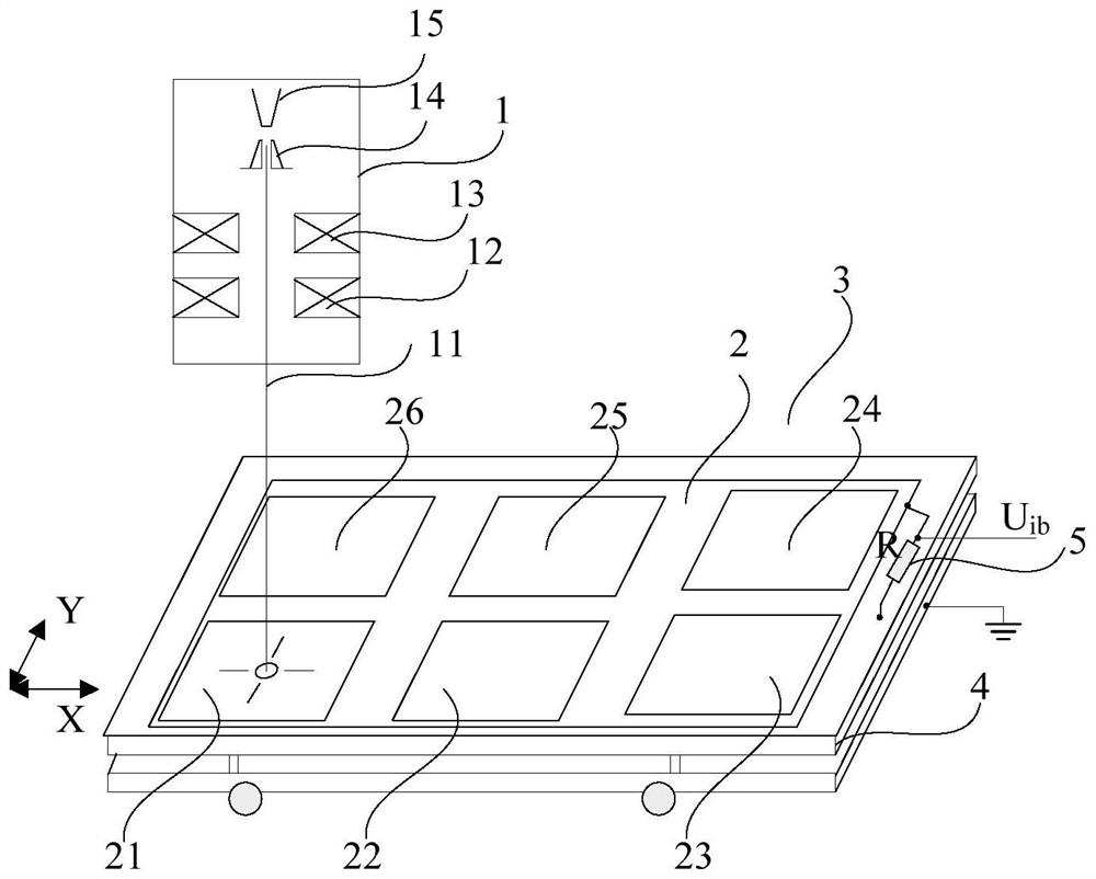
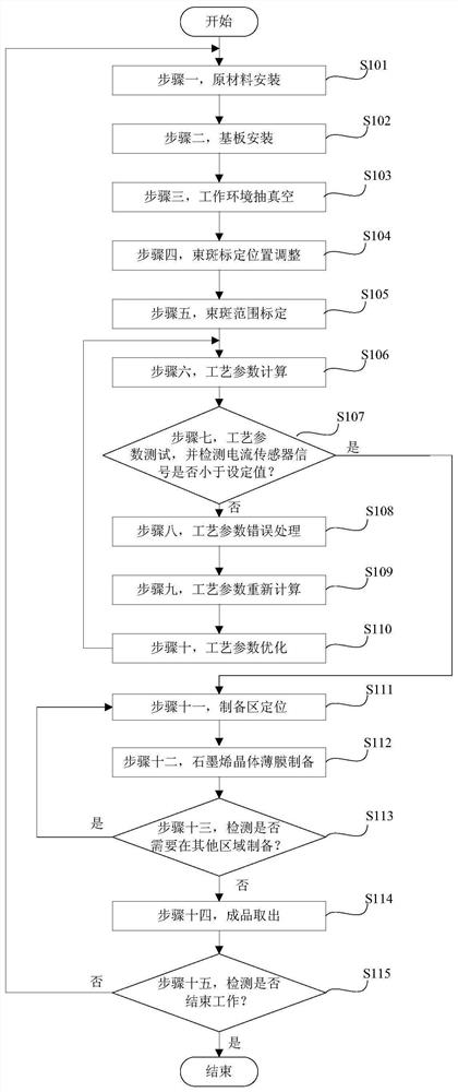
[0053] refer to Figure 1 ~ Figure 3 , a kind of electron beam scanning method of the present invention prepares graphene crystal film, detailed steps are as follows:
[0054] Step 1 S101, raw material installation: laying one or more carbon polymer films with length L and width W on the preparation areas 23-26 of the metal substrate 2;
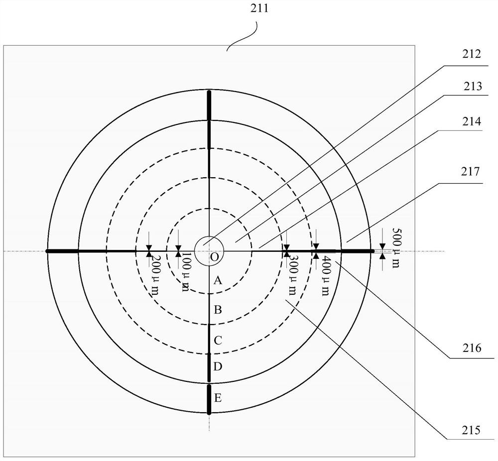
[0055] In this step, the metal substrate 2 is provided with a beam calibration area 21 and a process parameter testing area 22. The beam calibration area 21 is a ceramic sheet 211 provided with a beam intensity calibration hole 212 and a beam spot size range calibration area. The area covered on the metal substrate 2, the beam spot size range calibration area is on the ceramic sheet 211 on the ring concentric with the beam intensity calibration hole 212, and the corresponding width, Slots of the same length. The process parameter test area 22 is an area covered with a carbon polymer film of the same material as the preparation area 23-26 ne...
Embodiment 2
[0074] It needs to be clarified that in the present invention, whether the beam spot size range is accurately determined is related to the overlapping ratio of the beam spots of two adjacent rows of electron beam scanning, which will affect the quality of the graphene crystal film prepared by electron beam scanning. When scanning, the circular scanning range of the electron beam scanning covers the calibration area of 100 μm to 500 μm successively, and at the same time adjust the focusing current I of the focusing coil 13 of the electron gun f , the beam spot diameter D of the electron beam 11 is set to a given range, and the focusing current I of the electron gun focusing coil 13 is recorded f1 , after adjusting the focus current, turn off the beam current output of electron gun 1.
[0075] In the present invention, the beam calibration area 21 is set on the substrate 2, and the method for determining the size range of the beam spot is as follows:
[0076] In the beam inte...
Embodiment 3
[0087] In this embodiment, a graphene crystal film is prepared by taking a polyimide film covered with a thickness of 125 μm in any preparation area as an example. The height H of the preparation area from the beam outlet of the electron gun 1 is 200mm to 300mm, and the working voltage U of the electron gun 1 hv Set to -20kV, beam current I b Set to 3mA, electron gun 1 focusing coil 13 focusing current 560mA, the beam spot of the electron beam is controlled within the range of 500μm.
[0088] It should be noted that, in the present invention, the origin of the electron beam 11 scanning coordinates can be set at any apex position or central point of the preparation area used. If the origin of the electron beam 11 scanning coordinates is different, the X direction, The current value set by the Y-direction drive circuit is positive and negative. According to the electron beam 11 scanning coordinate origin setting position, judge the quadrant of the processed polyimide film in th...
PUM
| Property | Measurement | Unit |
|---|---|---|
| Thickness | aaaaa | aaaaa |
Abstract
Description
Claims
Application Information
 - R&D
- Intellectual Property
- Life Sciences
- Materials
- Tech Scout
- Unparalleled Data Quality
- Higher Quality Content
- 60% Fewer Hallucinations
Browse by: Latest US Patents, China's latest patents, Technical Efficacy Thesaurus, Application Domain, Technology Topic, Popular Technical Reports.
© 2025 PatSnap. All rights reserved.Legal|Privacy policy|Modern Slavery Act Transparency Statement|Sitemap|About US| Contact US: help@patsnap.com