Supercharge Your Innovation With Domain-Expert AI Agents!

Ultrathin large-area solder ball printing process adopting polyimide

A polyimide, large-area technology, applied in the field of semiconductor technology, can solve the problems of bending or fragmentation, difficult process, decomposition and damage, etc., and achieve the effect of reducing process difficulty and process cost.

Active Publication Date: 2021-01-15
绍兴同芯成集成电路有限公司
View PDF5 Cites 2 Cited by
  • Summary
  • Abstract
  • Description
  • Claims
  • Application Information

AI Technical Summary

Problems solved by technology

[0002] In order to overcome the problem of wafer bending or fragmentation in ultra-thin wafer production engineering, in addition to using glass slides (printing solder balls on the front of the glass slide requires opening windows on the glass slide, the process is more difficult), polymers can also be used. Imide achieves the effect of stress buffering on the front and back respectively, and polyimide can remain on the element as a protective layer, and can be directly developed by photosensitive polyimide material to form a pattern, but polyimide Amine is a polymer material, and it is not suitable for high-vacuum manufacturing process after it is attached to the wafer. There will be no outgassing problem unless the bond is completely induced and solidified, and polyimide cannot withstand high temperature steps exceeding (450°C to 500°C). Otherwise, decomposition and damage will occur;

Method used


Image

  • Ultrathin large-area solder ball printing process adopting polyimide
  • Ultrathin large-area solder ball printing process adopting polyimide

Examples


Embodiment 1

[0046] An ultra-thin large-area solder ball printing process using polyimide, comprising the following steps:

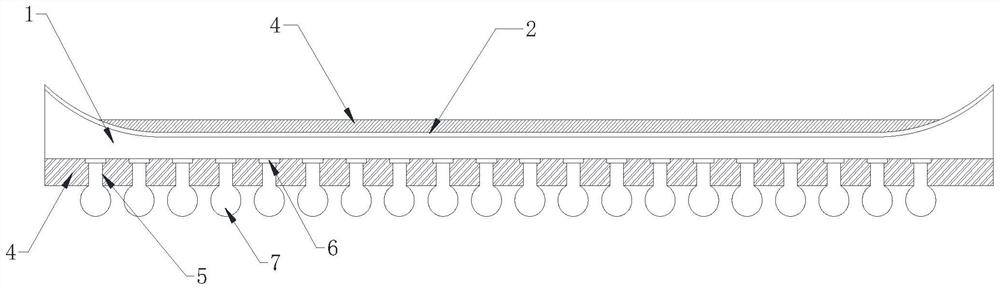
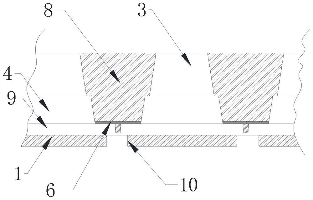
[0047] S1: Complete the contact hole of MOSFET or IGBT wafer 1 that has completed the front ILD process, and form a plug with W-CVD filling and CMP planarization. When the contact size is large, directly and continuously use Ti / Ni / Cu UBM metal contact holes , and generate a sputtered layer 2 on the surface of the wafer 1;

[0048] S2: Wafer 1 completes the lithography process to form UBM PAD 6 and photoresist layer 3, such as figure 1 , figure 2 As shown, wet etching removes the metal stack in the area outside the photoresist, and completes the formation of the UBM PAD 6 area before solder ball printing;

[0049] S3: Coating polyimide 4 on the front side, performing a lithography process to form the edge of the UBM PAD 6, but exposing the second window 10 that is printed with a large area of ​​solder balls in the middle of the UBM;

[0050] S4: complete the bonding...

Embodiment 2

[0059] An ultra-thin large-area solder ball printing process using polyimide, comprising the following steps:

[0060] S1: Complete the contact hole of MOSFET or IGBT wafer 1 that has completed the front ILD process, and form a plug with W-CVD filling and CMP planarization. When the contact size is large, directly and continuously use Ti / Ni / Cu UBM metal contact holes , and generate a sputtered layer 2 on the surface of the wafer 1;

[0061] S2: Wafer 1 completes the lithography process to form UBM PAD 6 and photoresist layer 3, such as figure 1 , figure 2 As shown, wet etching removes the metal stack in the area outside the photoresist, and completes the formation of the UBM PAD 6 area before solder ball printing;

[0062] S3: Coating polyimide 4 on the front side, performing a lithography process to form the edge of the UBM PAD 6, but exposing the second window 10 that is printed with a large area of ​​solder balls in the middle of the UBM;

[0063] S4: complete the bondi...


PUM


Abstract

The invention discloses an ultrathin large-area solder ball printing process adopting polyimide, which comprises the following steps of: generating a sputtering coating on the surface of a wafer, carrying out a lithography process on the wafer to form a UBM PAD and a photoresist layer, coating the polyimide on the front surface, bonding / curing the polyimide, turning over the wafer, grinding and etching, after the lithography process of the back surface element of the wafer is completed, completing polyimide coating thick film coating of the back surface, wafer overturning to the front surface,thick film photoresist pattern manufacturing at the opening of the UBM PAD, solder paste printing and filling into the first window, then carrying out photoresist removing, soldering flux spraying, heating reflux forming of solder balls and wafer front surface soldering plate completing, overturning to the back surface of the wafer, removing the polyimide coating thick film on the back surface, removing the insulating layer, and carrying out a back surface metal evaporation process. According to the invention, polyimide is used; and compared with a glass carrier, polyimide has the advantagesthat wafer grinding, etching and lithography processes can be better completed under the assistance of photosensitivity and a stress buffer function, and the process difficulty is reduced.

Description

technical field [0001] The invention relates to the field of semiconductor technology, in particular to an ultra-thin and large-area tin ball printing process using polyimide. Background technique [0002] In order to overcome the problem of wafer bending or fragmentation in ultra-thin wafer production engineering, in addition to using glass slides (printing solder balls on the front of the glass slide requires opening windows on the glass slide, the process is more difficult), polymers can also be used. Imide achieves the effect of stress buffering on the front and back respectively, and polyimide can remain on the element as a protective layer, and can be directly developed by photosensitive polyimide material to form a pattern, but polyimide Amine is a polymer material, and it is not suitable for high-vacuum manufacturing process after it is attached to the wafer. There will be no outgassing problem unless the bond is completely induced and solidified, and polyimide canno...

Claims


Application Information

Patent Timeline
Patent Type & Authority Applications(China)
IPC IPC(8): H01L21/683H01L21/60
CPCH01L21/6835H01L24/11H01L24/94H01L2221/68372H01L2221/68381H01L2224/113H01L2224/1131
Inventor 严立巍文锺符德荣
Owner 绍兴同芯成集成电路有限公司
Features
  • R&D
  • Intellectual Property
  • Life Sciences
  • Materials
  • Tech Scout
  • Unparalleled Data Quality
  • Higher Quality Content
  • 60% Fewer Hallucinations
Learn More