Double-sided heat dissipation power semiconductor module and manufacturing method thereof

A power semiconductor, double-sided heat dissipation technology, applied in the fields of semiconductor/solid-state device manufacturing, semiconductor devices, semiconductor/solid-state device components, etc., can solve the problems of low production yield and inconsistent chip height, and reduce life and reliability. , uniform distribution, the effect of reducing contact resistance

Pending Publication Date: 2021-01-26
ZHEJIANG UNIV
View PDF0 Cites 0 Cited by
  • Summary
  • Abstract
  • Description
  • Claims
  • Application Information

AI Technical Summary

Problems solved by technology

[0007] In order to solve the problems of the existing double-sided heat dissipation power semiconductor module chips with inconsistent chip heigh

Method used


Image

  • Double-sided heat dissipation power semiconductor module and manufacturing method thereof
  • Double-sided heat dissipation power semiconductor module and manufacturing method thereof
  • Double-sided heat dissipation power semiconductor module and manufacturing method thereof

Examples


Embodiment Construction

[0032] Embodiments of the present disclosure will be described in detail below in conjunction with the accompanying drawings.

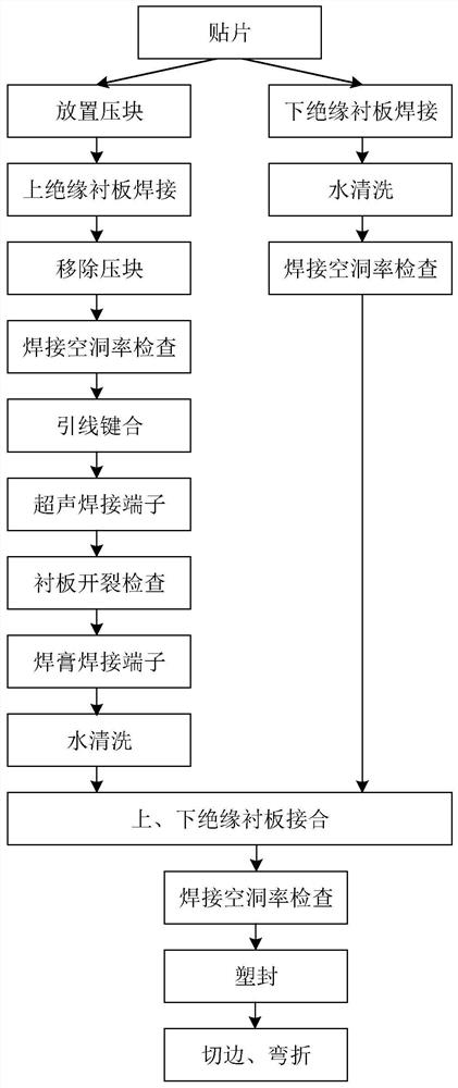
[0033] A double-sided heat dissipation power semiconductor module manufacturing method proposed by the present invention adopts the process of "bonding + secondary welding" for welding the power / signal terminals, which limits the bonding parameters selected by the power / signal terminals, and the selection is omitted. Small bonding parameters ensure that the insulating liner will not crack due to excessive bonding parameters, and the subsequent secondary welding process steps further strengthen the welding strength, avoiding the traditional welding process using high-energy bonding parameters to cause cracking of the insulating liner , and it is necessary to adjust the process parameters by trial and error before producing a certain module, which takes a lot of time and cost, and there will be defects of low production yield.

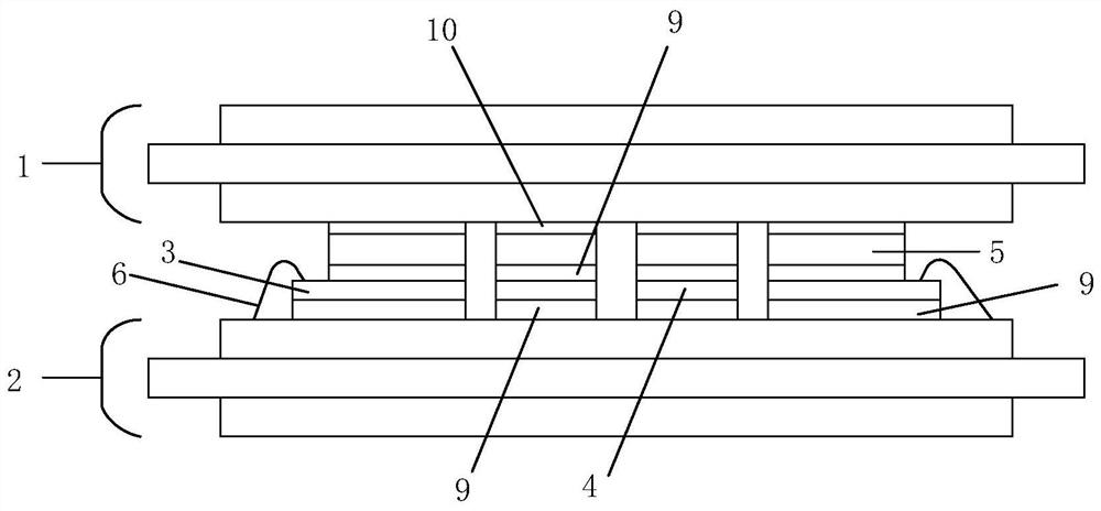
[0034] The structure of ...


PUM

PropertyMeasurementUnit
Thicknessaaaaaaaaaa

Abstract

The invention discloses a double-sided heat dissipation power semiconductor module and a manufacturing method thereof, and belongs to the technical field of semiconductors. The semiconductor module iscomposed of an upper-layer insulating lining plate, a lower-layer insulating lining plate, a power semiconductor chip, a metal gasket, an aluminum wire, a power terminal and a signal terminal. The power semiconductor chip is jointed with the lower-layer insulating lining plate through a preformed soldering lug, and after the power semiconductor chip is placed above the preformed soldering lug, reflow soldering is carried out after a prestress pressing block is applied to the surface of the power semiconductor chip; the power terminals and the signal terminals are welded with the lower-layer insulating lining plate through ultrasonic bonding, and reflow soldering is carried out after soldering paste is coated around pins of the power terminals and the signal terminals. According to the manufacturing method of the double-sided heat dissipation power semiconductor module provided by the invention, the consistency of the height of the welded chip is improved, the welding void ratio is reduced, the connection strength between the terminal and the insulating lining plate is ensured, and the problem of cracking of a ceramic layer of the insulating lining plate caused by an ultrasonic bonding process is solved.

Description

technical field [0001] The present disclosure relates to the technical field of semiconductors, in particular to a double-sided heat dissipation power semiconductor module and a manufacturing method. Background technique [0002] Complex and changeable operating conditions require electric vehicles to have the characteristics of strong power and high reliability. The power semiconductor module in the electric drive traction inverter is the main factor determining the power output capability and service life of electric vehicles. After decades of development, power semiconductor chips have higher current density, reliability and price advantages, as well as lower power consumption. At the same time, due to the limited current-carrying capacity of a single power semiconductor chip, multiple chips need to be packaged in parallel before use. Therefore, the packaging structure is a major factor affecting the power output capability of the electric vehicle chip and the reliability...

Claims


Application Information

Patent Timeline
IPC IPC(8): H01L21/60H01L21/603H01L21/607H01L23/488H01L23/367
CPCH01L24/80H01L23/488H01L23/367H01L2224/80815H01L2224/80894H01L21/607H01L21/603H01L2224/73265H01L2224/32225H01L2224/48091H01L2224/48227H01L2224/0603H01L2924/00014H01L2924/00
Inventor 罗皓泽高洪艺周宇谢刚李武华何湘宁
Owner ZHEJIANG UNIV
Why Eureka
Try Eureka