Solar cell
A solar cell and substrate technology, applied in the field of solar cells, can solve problems affecting the conversion efficiency of solar cells, etc., and achieve the effects of optimizing the resistance of the back electrode, small thickness of the back electrode, and small resistivity
- Summary
- Abstract
- Description
- Claims
- Application Information
AI Technical Summary
Problems solved by technology
Method used
Image
Examples
preparation example Construction
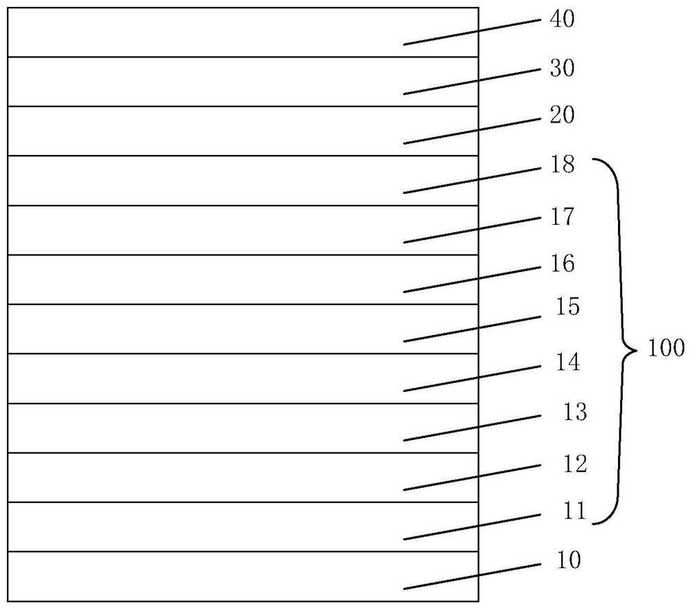
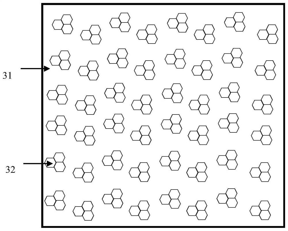
[0034]According to another aspect of the present invention, there is also provided a method for preparing the above-mentioned solar cell, comprising the following steps: forming an epitaxial layer 100 on a substrate 10; growing graphene on the epitaxial layer 100 and doping graphene quantum dots Graphene and graphene quantum dots are compounded to form a diffusion barrier layer 30; on the diffusion barrier layer 30, a back metal layer 40 is formed.
[0035] Specifically, the preparation process of the above-mentioned solar cell of the present invention may include the following processes:
[0036] 1) GaAs substrate 10 is placed in MOCVD equipment, under H 2 Under the protection of raising temperature to reaction temperature;
[0037] 2) Ga source and As source are introduced, GaAs is grown on GaAs substrate to obtain buffer layer 11, and the growth temperature is 800-1200°C;
[0038] 3) cut off the Ga source, feed the Al source, grow AlAs on the buffer layer 11 to obtain the...
Embodiment 1
[0051] This embodiment provides a method for preparing a solar cell, comprising the following steps:
[0052] On the GaAs substrate, a GaAs buffer layer with a thickness of 1000nm, an AlAs sacrificial layer with a thickness of 15nm, and an n-type GaAs ohmic contact layer with a thickness of 60nm (Si doped with a doping concentration of 5×10 17 cm -3 ), an AlInP top cell window layer with a thickness of 30nm, an n-type GaAs absorber layer with a thickness of 2400nm, a GaAs / AlGaAs PN junction with a thickness of 100nm, an AlGaAs bottom cell window layer with a thickness of 250nm, and a C-doped p Type AlGaAs ohmic contact layer (C-doped, doping concentration is 1×10 18 cm -3 ), an Ag light reflective layer with a thickness of 100 nm, a diffusion barrier layer 30 with a thickness of 10 nm, and a Cu back metal layer with a thickness of 3000 nm.
[0053] Wherein, the diffusion barrier layer is a graphene composite material layer, including graphene and graphene quantum dots doped...
Embodiment 2
[0056] The difference between the solar cell provided in this embodiment and Embodiment 1 is:
[0057] The thickness of the back metal layer is 2500nm.
PUM
| Property | Measurement | Unit |
|---|---|---|
| size | aaaaa | aaaaa |
| thickness | aaaaa | aaaaa |
| thickness | aaaaa | aaaaa |
Abstract
Description
Claims
Application Information


