High-hardness Cu-based material containing interface layers and preparation method thereof

An interface layer, high hardness technology, applied in metal material coating process, coating, ion implantation plating and other directions, can solve the problems of difficulty in practical engineering, low hardness and strength of Cu, achieve high hardness, improve mechanical Performance, simple process effect

Pending Publication Date: 2021-02-05
HEBEI UNIV OF TECH
View PDF3 Cites 0 Cited by
  • Summary
  • Abstract
  • Description
  • Claims
  • Application Information

AI Technical Summary

Problems solved by technology

[0004] The present invention aims at the problem that pure Cu is low in hardness and strength as a structural material, and is difficult to be applied to practical engineering, etc., and provides a high-hardness Cu-based material containing an interface layer and a preparation method thereof

Method used


Image

  • High-hardness Cu-based material containing interface layers and preparation method thereof
  • High-hardness Cu-based material containing interface layers and preparation method thereof
  • High-hardness Cu-based material containing interface layers and preparation method thereof

Examples


Embodiment 1

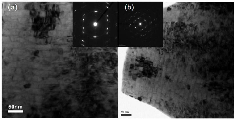
[0035] Cu-based composites with Nb interfacial layer were prepared by high-vacuum multi-chamber magnetron sputtering thin film deposition system TRP450.

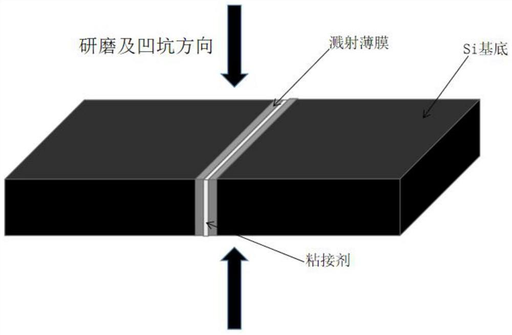
[0036] Alcohol is used to pre-clean the silicon wafer, and the pre-cleaned silicon wafer is placed on the reverse sputtering target, and the pressure of argon gas is 0.4Pa, and the reverse sputtering time is 10 minutes; the reverse sputtering power is 80W.

[0037] Place the silicon wafer in the sputtering chamber, preset parameters: the argon pressure in the sputtering chamber is 0.4Pa, the sputtering temperature is 25°C, the bias voltage is -100V, and the rotation speed of the sample stage is 10r / min.

[0038]Cu and Nb two kinds of targets are sputtered alternately, the magnetron power of fixed Cu power supply is 20W, and the magnetron power of Nb power supply is 60W. Alternate growth of Cu layer and Nb layer film. The sputtering time of the Cu target is fixed at 180s, and the sputtering time of the Nb target is 10s.

[...

Embodiment 2

[0045] Cu-based composites with Nb interfacial layer were prepared by high-vacuum multi-chamber magnetron sputtering thin film deposition system TRP450.

[0046] Alcohol is used to pre-clean the silicon wafer, and the pre-cleaned silicon wafer is placed on the reverse sputtering target, and the pressure of argon gas is 0.4Pa, and the reverse sputtering time is 10 minutes; the reverse sputtering power is 80W.

[0047] Place the silicon wafer in the sputtering chamber, preset parameters: the argon pressure in the sputtering chamber is 0.4Pa, the sputtering temperature is 25°C, the bias voltage is -100V, and the rotation speed of the sample stage is 10r / min.

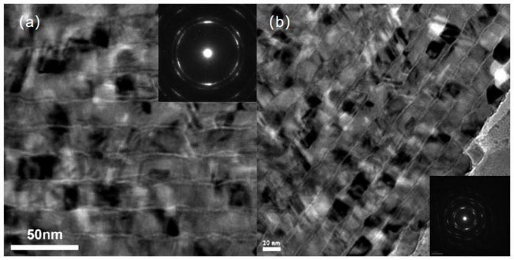
[0048] Cu and Nb two kinds of targets are sputtered alternately, the magnetron power of fixed Cu power supply is 20W, and the magnetron power of Nb power supply is 60W. Alternate growth of Cu layer and Nb layer film. The sputtering time of the Cu target is fixed at 180s, and the sputtering time of the Nb target is 7s.

[...

Embodiment 3

[0055] Cu-based composites with Nb interfacial layer were prepared by high-vacuum multi-chamber magnetron sputtering thin film deposition system TRP450. .

[0056] Alcohol is used to pre-clean the silicon wafer, and the pre-cleaned silicon wafer is placed on the reverse sputtering target, and the pressure of argon gas is 0.4Pa, and the reverse sputtering time is 10 minutes; the reverse sputtering power is 80W.

[0057] Place the silicon wafer in the sputtering chamber, preset parameters: the argon pressure in the sputtering chamber is 0.4Pa, the sputtering temperature is 25°C, the bias voltage is -100V, and the rotation speed of the sample stage is 10r / min.

[0058] Cu and Nb two kinds of targets are sputtered alternately, the magnetron power of fixed Cu power supply is 20W, and the magnetron power of Nb power supply is 60W. Alternate growth of Cu layer and Nb layer film. The sputtering time of the Cu target is fixed at 180s, and the sputtering time of the Nb target is 5s. ...


PUM

PropertyMeasurementUnit
thicknessaaaaaaaaaa
thicknessaaaaaaaaaa
hardnessaaaaaaaaaa

Abstract

The invention discloses a high-hardness Cu-based material containing interface layers and a preparation method thereof. The material comprises Cu matrix layers and the interface layers, wherein the Cumatrix layers and the interface layers are alternately superposed; an initial layer and a final layer are Cu layers; the interlayer modulation ratio is 10:1-50:1; the interface layers are Nd, Zr, Ag,CuZr amorphous and CuNb amorphous; the thicknesses of the Cu layers are the same; the thickness range of the single Cu layer is 5-50 nm; the thicknesses of the interface layers are the same; and thethickness range of the single interface layer is 0.5-2 nm. The prepared high-hardness Cu-based material has such mechanical properties as higher hardness; and the interface layers generate no side effect on the matrix Cu. The preparation method of the Cu-based material is simple in production process, low in cost and suitable for industrial application and automatic batch production, and has unique structure and performance advantages in such fields as microelectronic components, power transmission devices, integrated circuits and printed circuits.

Description

Technical field: [0001] The invention relates to the technical field of nanometer metal thin film materials, in particular to a high-hardness Cu-based material containing an interface layer and a preparation method thereof. Background technique: [0002] Cu has excellent electrical conductivity, corrosion resistance, and ductility, and is relatively inexpensive. However, due to the extremely poor strength and hardness of Cu, its application in industrial production, especially in the field of microelectronics is limited. However, through the design of the interface layer, adding a 1-2nm heterogeneous interface layer in the Cu matrix to change the interface structure will significantly improve the mechanical properties such as the overall strength and hardness of the material, and because the thickness of the interface layer is much smaller than the thickness of the Cu layer of the matrix, so The introduced interfacial layer basically does not destroy the excellent propertie...

Claims


Application Information

Patent Timeline
Patent Type & Authority Applications(China)
IPC IPC(8): C23C14/35C23C14/16C22C9/00C22C1/00
CPCC23C14/352C23C14/165C22C9/00C22C1/00C22C2204/00
Inventor 郑士建姜水淼明开胜王静
Owner HEBEI UNIV OF TECH
Why Eureka
Try Eureka