Polishing pad and preparation method and application thereof

A polishing pad and polishing layer technology, which is applied in the direction of grinding/polishing equipment, manufacturing tools, metal processing equipment, etc., can solve the defects of polishing layer adaptability, different degrees of wafer surface grinding, and difficulty in controlling the flatness of wafer grinding issues with uniformity

Active Publication Date: 2021-02-09
HUBEI DINGHUI MICROELECTRONICS MATERIALS CO LTD +1
View PDF6 Cites 4 Cited by
  • Summary
  • Abstract
  • Description
  • Claims
  • Application Information

AI Technical Summary

Problems solved by technology

[0006] In order to solve the existing polishing technology, the linear speed along the radius direction of the polishing pad gradually increases, and the grinding removal rate gradually increases, and then the defects caused by different grinding degrees are formed on the surface of the wafer; the more layers of soft and hard pads are laminated , the more variables there are in the physical properties of the polishing layer pad, the more difficult it is to control the flatness and uniformity of wafer grinding; the adaptability of the grinding disc and polishing liquid to the polishing layer of different materials causes defects

Method used


Image

  • Polishing pad and preparation method and application thereof
  • Polishing pad and preparation method and application thereof
  • Polishing pad and preparation method and application thereof

Examples


preparation example Construction

[0056] Preparation of polishing layer:

[0057] The raw material of polishing layer comprises each component of following mass fraction: the prepolymer of 100 parts of isocyanate termination, the curing agent of 20 parts and the hollow microsphere of 2.0 parts; Wherein, the prepolymer of described isocyanate termination is made of toluene di It is obtained by reacting isocyanate and polytetrahydrofuran; the curing agent is MOCA, and the MOCA is 3,3-dichloro-4,4-diaminodiphenylmethane; the model of the hollow microsphere is 551DE20d42.

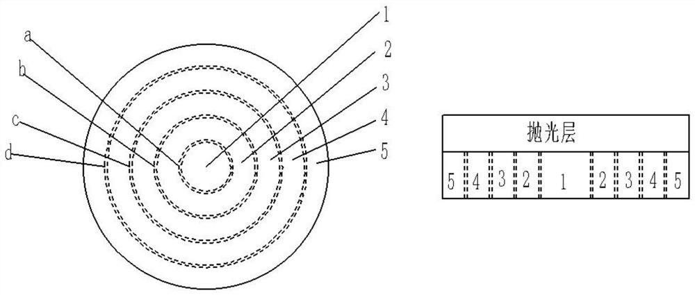
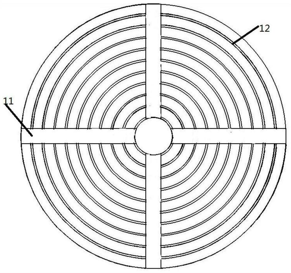
[0058] In the present invention, preferably, radial grooves are further provided on the polishing layer, and the radial grooves are used to receive polishing fluid during polishing. Wherein, the width of the radial groove is preferably 0.1-0.6 cm, more preferably 0.2-0.4 cm.

[0059] Specific steps:

[0060] Step (1): the treatment of the isocyanate-terminated polyurethane prepolymer (or prepolymer for short); the specific operations are as f...

Embodiment 1-10

[0065] Step (1): 100 parts of prepolymer with NCO% content of 7.74%-9.45%, 16.7 parts of BDO, 50 parts of DMF solution, after mixing evenly, react at 80°C for 200min to obtain the required polyurethane solution.

[0066] Step (2): Make the density 0.10-0.30g / cm 3 The impregnated viscosity of the polyester non-woven fabric is 6000-15000cp in the DMF (dimethylformamide) solution of polyurethane for 100-300s. Generally speaking, the density of the buffer layer can be adjusted by the density of the non-woven fabric and the viscosity of the polyurethane DMF solution. Polyurethane DMF solution is easier to impregnate low-density non-woven fabrics to form high-density cushions: after immersion in the coagulation tank of 5% DMF aqueous solution for 300s to shape TPU; after immersion in water washing tank for 200s, the large Part of the DMF solution was washed off; and then placed in a tunnel furnace at 150°C for 600s to remove water and DMF solution.

[0067] Step (3): The buffer pad i...


PUM


Abstract

The invention discloses a polishing pad and a preparation method and application thereof. The polishing pad is provided with a buffer layer and a polishing layer, wherein the buffer layer is formed bycombined pieces with different compression ratios and resilience rates, and the polishing layer is overlapped on the buffer layer; and a center circle center buffer area, one or more middle annular buffer areas sequentially arranged around the center buffer area and an outer edge annular buffer area arranged around the middle buffer areas are formed by the different combined pieces. The compression ratios and the resilience rates of the combined pieces of the buffer layer are different in the direction from the center of the polishing pad to the outer edge of the polishing pad, in the mechanical polishing process, the wear rate of the combined pieces is basically kept consistent, and therefore the surface of a wafer to be polished can become flat, and the flattening efficiency is high.

Description

technical field [0001] The invention relates to a polishing pad and its preparation method and application. Background technique [0002] A semiconductor chip is mainly composed of isolation structures, transistors, metal layers and dielectric layers. In the chip manufacturing process, before the new structure is stacked, the original structure needs to be planarized to obtain a globally planarized plane. This process is called chemical mechanical polishing (CMP). The chemical mechanical polishing pad is a circular sheet-shaped composite material with a diameter of 50-100cm, which is an important part of the CMP system and the main consumable of CMP. The surface structure and structure of the chemical mechanical polishing pad directly affect the performance of the polishing pad, and then affect the CMP process and processing effect. [0003] In a typical CMP process, a wafer is mounted upside down on a carrier of a CMP tool, and force pushes the carrier and wafer down towa...

Claims


Application Information

Patent Timeline
Patent Type & Authority Applications(China)
IPC IPC(8): B24D3/28B24D11/00B24D11/02B24D11/04B24D18/00
CPCB24D3/28B24D11/001B24D11/02B24D11/04B24D18/00
Inventor 王腾罗乙杰王磊刘敏杨浩
Owner HUBEI DINGHUI MICROELECTRONICS MATERIALS CO LTD
Why Eureka
Try Eureka