Film acoustic resonator and manufacturing method thereof

A technology of acoustic wave resonator and thin-film acoustic wave, applied in the direction of electrical components, impedance network, etc., can solve the problems of reducing equipment performance, electromagnetic interference, and small ratio, and achieve the effect of improving structural strength and suppressing external electromagnetic radiation

Pending Publication Date: 2021-02-09
NINGBO SEMICON INT CORP
View PDF0 Cites 6 Cited by
  • Summary
  • Abstract
  • Description
  • Claims
  • Application Information

AI Technical Summary

Problems solved by technology

[0003] In the existing mass-produced thin-film acoustic wave resonators, the electromagnetic waves generated by the densely arranged resonator units during operation will cause electromagnetic interference to the outside and reduce the performance of the equipment
At the same time, the high acoustic impedance material of the Bragg reflection layer...

Method used


Image

  • Film acoustic resonator and manufacturing method thereof
  • Film acoustic resonator and manufacturing method thereof
  • Film acoustic resonator and manufacturing method thereof

Examples


Embodiment 1

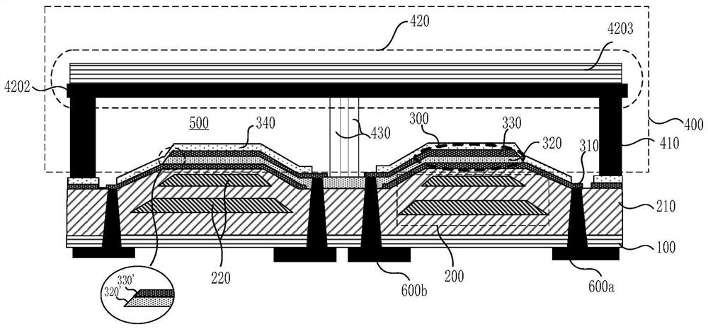
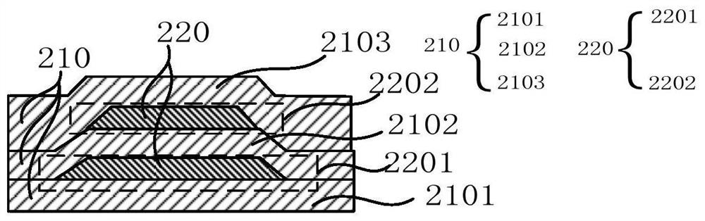
[0033] This embodiment provides a thin film acoustic resonator, wherein the thin film acoustic resonator is a solid assembly type resonator, figure 1 A schematic structural view of the thin film acoustic resonator of Embodiment 1 is shown, figure 2 A schematic structural diagram showing the structure of the Bragg reflection layer of Embodiment 1, please refer to figure 1 with figure 2 , the thin film acoustic resonator consists of:

[0034] A first substrate 100 containing an acoustic reflection structure; (in this embodiment, the acoustic reflection structure is a Bragg reflection layer structure, and may be a cavity structure in other embodiments)

[0035] The acoustic wave resonator unit 300 (shown in the elliptical dotted line box), at least partly located on the acoustic reflection structure, the acoustic wave resonator unit 300 sequentially includes a first electrode 310, a piezoelectric layer 320 and a second electrode 330 from bottom to top;

[0036] The substrat...

Embodiment 2

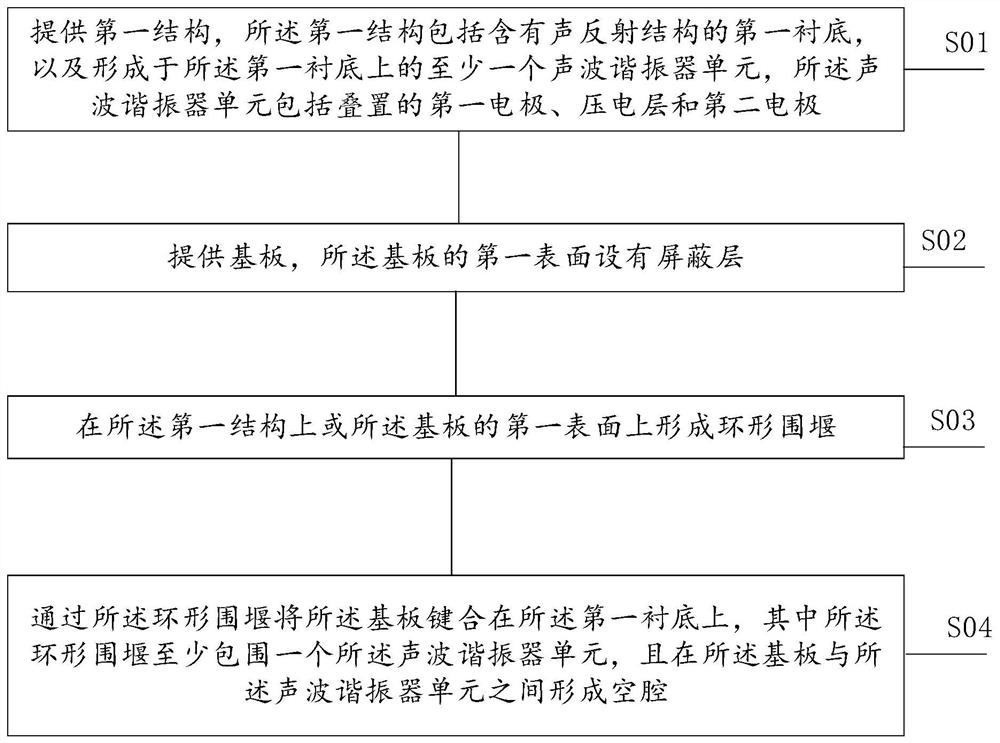
[0052] An embodiment of the present invention provides a method for manufacturing a thin-film acoustic wave resonator, please refer to image 3 , image 3 It is a flow chart of a manufacturing method of a thin film acoustic wave resonator according to an embodiment of the present invention, and the manufacturing method includes:

[0053] S01: Provide a first structure, the first structure includes a first substrate including an acoustic reflection structure, and at least one acoustic resonator unit formed on the first substrate, the acoustic resonator unit includes a stack The first electrode, the piezoelectric layer and the second electrode;

[0054] S02: providing a substrate, the first surface of the substrate is provided with a shielding layer;

[0055] S03: forming an annular cofferdam on the first structure or on the first surface of the substrate;

[0056] S04: Bond the substrate to the first substrate through the annular dam, wherein the annular dam surrounds at lea...


PUM


Abstract

The present invention provides a film acoustic resonator and a manufacturing method thereof, the film acoustic resonator comprising: a first substrate including an acoustic reflection structure; an acoustic resonator unit at least part of which is located on the acoustic reflection structure, and which sequentially comprises a first electrode, a piezoelectric layer and a second electrode which arestacked from bottom to top; and a substrate bonded with the first substrate through an annular cofferdam, wherein a cavity is formed between the substrate and the acoustic resonator unit, the cavityat least comprises one acoustic resonator unit therein, and at least one of the substrate and the annular cofferdam has an effect of shielding electromagnetic waves. According to the film acoustic resonator, the external propagation of electromagnetic waves generated by the resonator unit is effectively blocked or attenuated, so that the external electromagnetic radiation of the resonator unit isinhibited.

Description

technical field [0001] The invention relates to the field of semiconductor device manufacturing, in particular to a thin-film acoustic wave resonator and a manufacturing method thereof. Background technique [0002] The structure of the film bulk acoustic resonator is a layer of c-axis orientation (or z-axis orientation) piezoelectric film sandwiched between the upper and lower layers of metal electrodes to form a sandwich structure, an alternating radio frequency voltage is applied between the two electrodes, using The piezoelectricity of the material converts electrical energy into acoustic energy. The acoustic wave is reflected on the interface between the medium and the air, forming a standing wave oscillation between the two interfaces. At this time, the acoustic wave loss is the smallest, and it is converted into electrical energy by the inverse piezoelectric effect. . The sound wave excited by the film bulk acoustic resonator is a bulk acoustic wave, and its resonant...

Claims


Application Information

Patent Timeline
IPC IPC(8): H03H3/02H03H9/02
CPCH03H3/02H03H9/02
Inventor 张显良赵洪波李志超李萍
Owner NINGBO SEMICON INT CORP
Why Eureka
Try Eureka