Process for manufacturing metallized coating under wafer bump and coating structure thereof

A technology of under-bump metallization and manufacturing process, which is applied in the direction of metal material coating process, liquid chemical plating, superimposed layer plating, etc., and can solve the problems of electroless nickel plating, gold penetration, independent pad missing plating, and short circuit and other problems to achieve the effect of overcoming the constraints of line width and line spacing and the constraints of line conductivity

Active Publication Date: 2021-02-19
SHENZHEN CHENGGONG CHEM
View PDF7 Cites 1 Cited by
  • Summary
  • Abstract
  • Description
  • Claims
  • Application Information

AI Technical Summary

Problems solved by technology

However, as the lines become thinner and the spacing becomes smaller and smaller, the process of electroless nickel-gold plating is greatly challenged, because electroless nickel-plating gold is prone to permeation, resulting in short circuit of two independent lines, or easy to make independent Missi

Method used


Image

  • Process for manufacturing metallized coating under wafer bump and coating structure thereof
  • Process for manufacturing metallized coating under wafer bump and coating structure thereof
  • Process for manufacturing metallized coating under wafer bump and coating structure thereof

Examples


Embodiment Construction

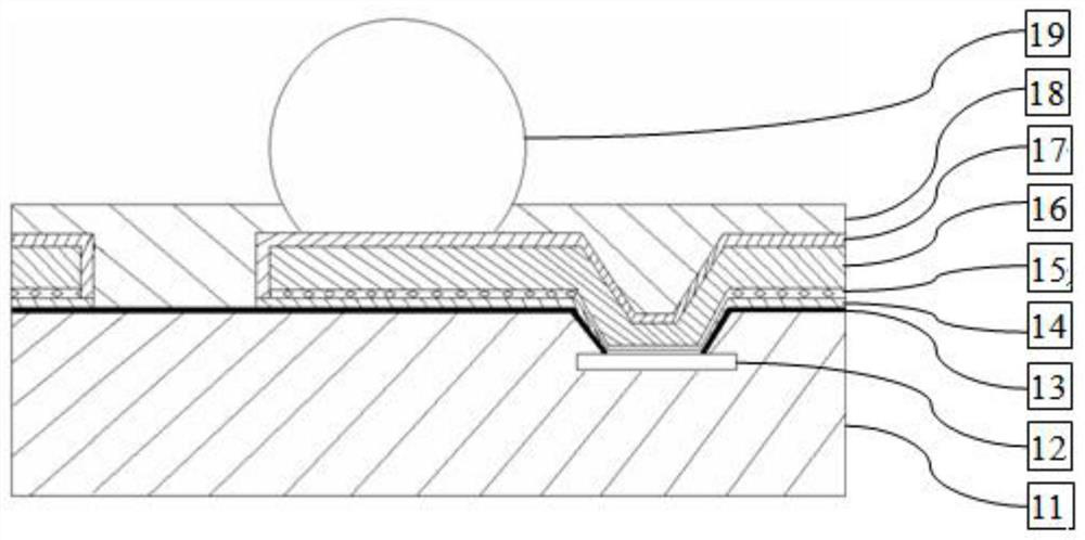
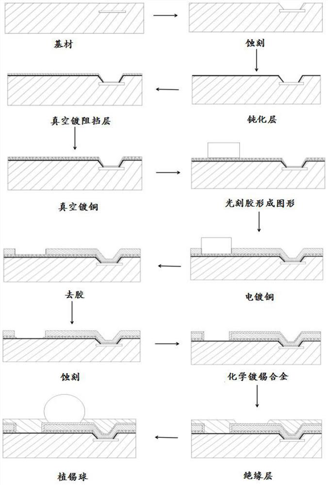
[0044] In order to express the present invention more clearly, the present invention will be further described below in conjunction with the accompanying drawings.

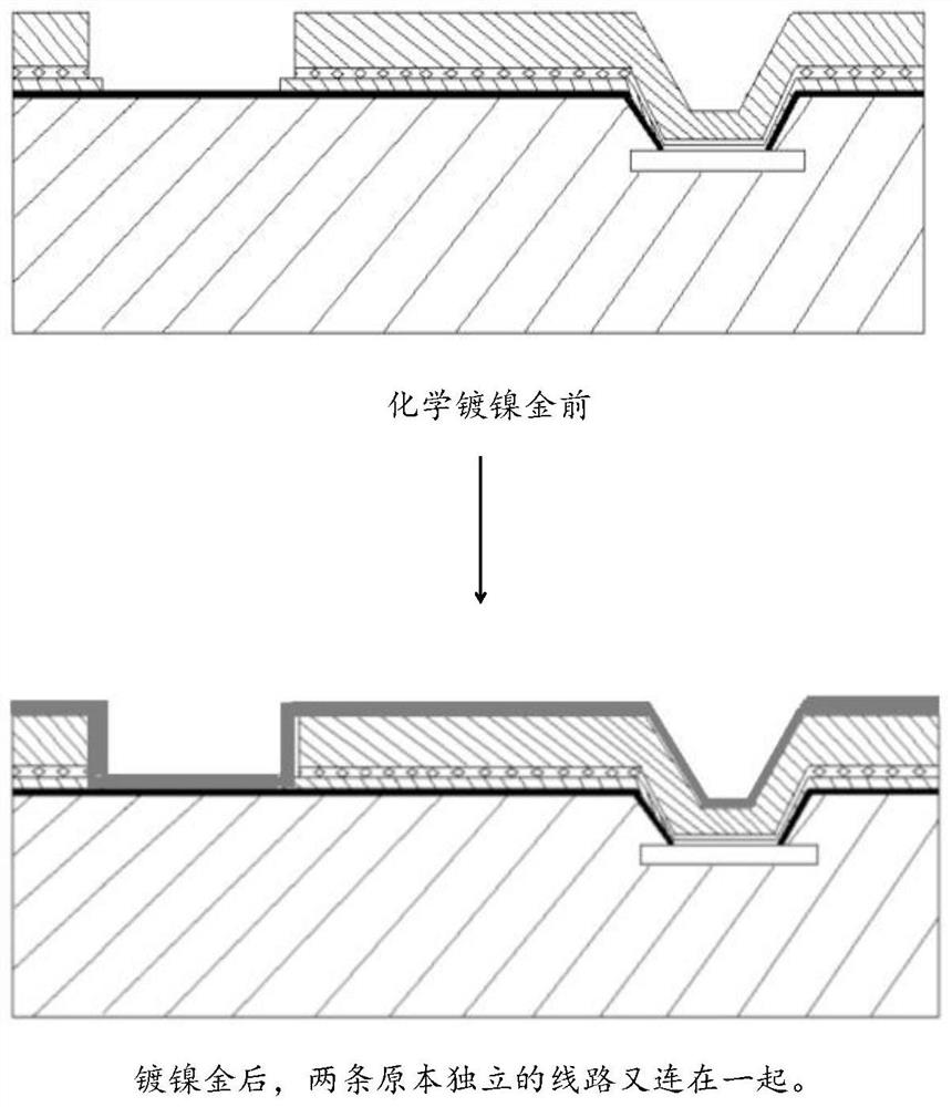
[0045] see Figure 1-2 , a coating manufacturing process for wafer under-bump metallization provided by the present invention, the base material 11 in the process is silicon or silicon carbide semiconductor; the base material surface is provided with a conductive circuit area and a non-conductive area, and a conductive After the substrate surface of the circuit area is recessed downward, an inverted wafer bump is formed on the substrate surface of the conductive circuit area;

[0046] The specific steps of the metallization coating process under the wafer bump are as follows: figure 2 ,Specifically:

[0047] Step 1, forming the metal electrode 12: the wafer substrate is etched to leak the electrodes inside the wafer, and the metal electrode 12 is formed at the bottom of the protruding part of the wafer bump;

...


PUM


Abstract

The invention discloses a process for manufacturing a metallized coating under a wafer bump and a coating structure thereof. A substrate in the process is a silicon or silicon carbide semiconductor; wherein a conductive circuit area and a non-conductive area are arranged on the surface of the substrate, and the conductive circuit area on the surface of the substrate sinks downwards to form an inverted wafer bump. The coating obtained through a chemical tin alloy plating process is a chemical replacement type coating, electrification is not needed, a traditional chemical auto-catalytic reactionis not needed, and only a replacement reaction is needed. The under bump metallization (UBM) and the redistribution line (RDL) obtained by the method provided by the invention not only can have binding property, but also have good weldability.

Description

technical field [0001] The invention relates to the technical field of integrated circuit packaging, in particular to a coating manufacturing process for metallization under wafer bumps and a coating structure thereof. Background technique [0002] With the increasing demand for high-performance and high-integration chips, the metal lines of the chip and its package are becoming smaller and smaller, so as to meet more I / O contacts and improve the computing performance of the chip. In particular, the RDL (redistribution) process of the fou-out process that has appeared in recent years has a line width and line spacing of 2 / 2 μm. [0003] The traditional advanced packaging is a flip-chip packaging process. The typical process is CSP (Chip Scale Package) packaging. The electrodes inside the chip are dispersed by RDL through the fan-in process, and then the balls are planted. This packaging and testing process is relatively traditional. Wire-bonded packaging saves a lot of spac...

Claims


Application Information

Patent Timeline
IPC IPC(8): H01L21/60H01L23/488C23C18/48C23C28/02C25D5/02
CPCH01L24/11H01L24/13C23C28/021C23C28/028C25D5/02C23C18/48H01L2224/11H01L2224/11462H01L2224/13111H01L2224/13147
Inventor 王江锋洪学平汪文珍
Owner SHENZHEN CHENGGONG CHEM
Why Eureka
Try Eureka