Deep ultraviolet LED with stepped electron blocking layer structure and preparation method

An electronic blocking layer and stepped technology, which is applied in the direction of circuits, electrical components, semiconductor devices, etc., can solve the problems of low efficiency of deep ultraviolet LEDs, alleviate the electron overflow effect, increase the equivalent barrier height, and improve luminous efficiency Effect

Inactive Publication Date: 2021-02-19
SUZHOU UVCANTEK CO LTD
View PDF9 Cites 4 Cited by
  • Summary
  • Abstract
  • Description
  • Claims
  • Application Information

AI Technical Summary

Problems solved by technology

[0005] The object of the present invention is to provide a deep ultraviolet LED with a stepped electron blocking layer structure and a preparation method, which is used to solve the problem of low efficiency of deep ultraviolet LEDs caused by the electron overflow effect in the prior art

Method used


Image

  • Deep ultraviolet LED with stepped electron blocking layer structure and preparation method
  • Deep ultraviolet LED with stepped electron blocking layer structure and preparation method
  • Deep ultraviolet LED with stepped electron blocking layer structure and preparation method

Examples


preparation example Construction

[0024] For the second solution proposed by the present invention, the steps of the method for preparing a deep ultraviolet LED with a stepped electron blocking layer structure include:

[0025] (1) Growth of AlN intrinsic layer. In this step, the low-temperature buffer layer in the AlN intrinsic layer is grown on the sapphire substrate under the condition of 400-800°C, with a thickness of 10-50nm; An intrinsic layer of AlN is grown on the layer, and the total thickness of the intrinsic layer of AlN is 500-4000nm.

[0026] (2) An n-type AlGaN electron injection layer is grown. In this step, the temperature is lowered to 800-1200°C, and an n-type AlGaN electron injection layer is grown on the AlN intrinsic layer, wherein the Al composition percentage is 20-90%, and the thickness is 500-4000nm.

[0027] (3) Growing the quantum well active layer. In this step, the temperature is lowered to 700°C to 1100°C, and a quantum well active layer is grown on the n-type AlGaN electron in...

Embodiment 1

[0034] In this example, the steps of preparing a deep ultraviolet LED with a stepped electron blocking layer structure are as follows:

[0035] (1) At 800°C, grow a low-temperature buffer layer in the AlN intrinsic layer on a sapphire substrate with a thickness of 10nm; raise the temperature to 1200°C, and grow an AlN intrinsic layer on the low-temperature buffer layer in the AlN intrinsic layer , the total thickness of the AlN intrinsic layer is 500 nm.

[0036] (2) Lower the temperature to 800°C, and grow an n-type AlGaN electron injection layer on the AlN intrinsic layer. The n-type AlGaN electron injection layer is specifically n-type Al 0.6 Ga 0.4 N, the thickness is 500-4000nm.

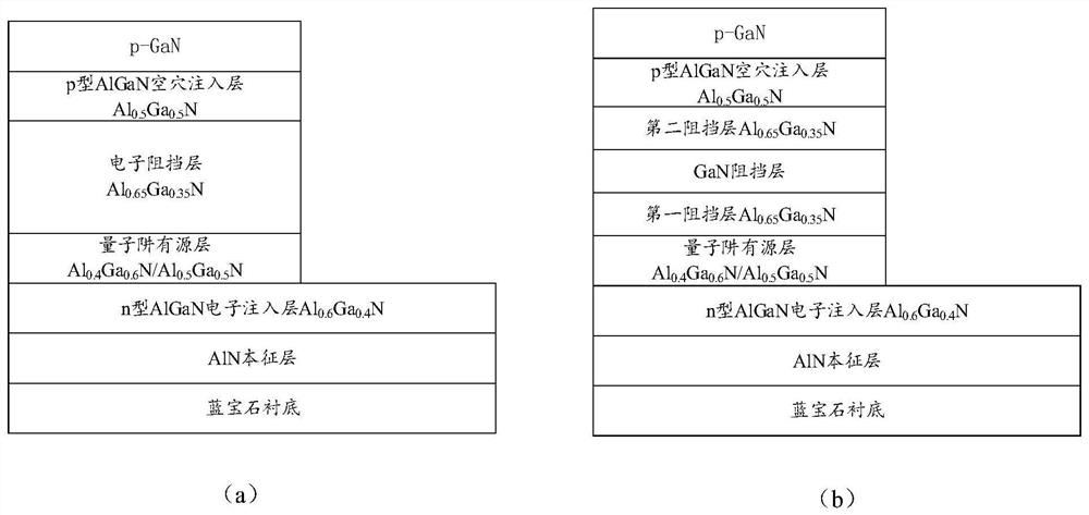
[0037] (3) Lower the temperature to 700°C, and grow a quantum well active layer on the n-type AlGaN electron injection layer. The quantum well active layer includes an AlGaN barrier layer and an AlGaN potential well layer. Specifically, the AlGaN barrier layer is Al 0.5 Ga 0.5 N, AlGaN poten...


PUM

PropertyMeasurementUnit
Thicknessaaaaaaaaaa
Thicknessaaaaaaaaaa
Thicknessaaaaaaaaaa

Abstract

The invention discloses a deep ultraviolet LED with a stepped electron blocking layer structure and a preparation method of the deep ultraviolet LED. The deep ultraviolet LED with the stepped electronblocking layer structure sequentially comprises a sapphire substrate, an AlN intrinsic layer, an n-type AlGaN electron injection layer, a quantum well active layer, a stepped electron blocking layer,a p-type AlGaN hole injection layer and a p-type GaN contact layer from bottom to top. The stepped electron blocking layer sequentially comprises a first AlGaN blocking layer, a GaN blocking layer and a second AlGaN blocking layer in the direction from the quantum well active layer to the p-type AlGaN hole injection layer, the Al component content percentage of the first AlGaN blocking layer is larger than the Al component content percentage of a potential barrier in the quantum well active layer, and the Al component content percentage of the second AlGaN barrier layer is greater than or equal to the Al component content percentage of the first AlGaN barrier layer. By introducing the stepped electron barrier layer structure, the equivalent barrier height of the electron barrier layer isincreased, and the electron overflow effect is relieved, so that the luminous efficiency of the deep ultraviolet LED is improved.

Description

technical field [0001] The invention relates to the field of semiconductor optoelectronics, in particular to a deep ultraviolet LED with a stepped electron blocking layer structure and a preparation method. Background technique [0002] As an outstanding representative of wide bandgap semiconductor materials, group III nitrides have realized high-efficiency blue-green light-emitting diodes (full name light-emitting diodes, referred to as LEDs), lasers and other solid-state light source devices, which are used in flat panel displays, white lighting, etc. The application has been a great success. In the past ten years, people expect to apply this high-efficiency luminescent material to the ultraviolet band to meet the increasing demand for ultraviolet light sources. According to its biological effects, the ultraviolet band can usually be divided into: long-wave ultraviolet (i.e. UVA, wavelength 320-400nm), medium-wave ultraviolet (i.e. UVB, wavelength 280-320nm), short-wave u...

Claims


Application Information

Patent Timeline
IPC IPC(8): H01L33/14H01L33/00
CPCH01L33/14H01L33/007
Inventor 张骏岳金顺梁仁瓅
Owner SUZHOU UVCANTEK CO LTD
Why Eureka
Try Eureka