Forming method of semiconductor device

A semiconductor and device technology, applied in the field of semiconductor device formation, can solve the problems of poor fin topography uniformity, fin field effect transistor threshold voltage shift, affecting the performance stability of fin field effect transistors, etc.

Pending Publication Date: 2021-03-05
SEMICON MFG INT (SHANGHAI) CORP +1
View PDF0 Cites 0 Cited by
  • Summary
  • Abstract
  • Description
  • Claims
  • Application Information

AI Technical Summary

Problems solved by technology

[0004] However, the fins formed by the current method, due to the poor uniformity of the edges and sidewalls of the fins, lead to the shift of the threshold voltage of the fin field effect transistor, which affects the stability of the performance of the fin field effect transistor

Method used


Image

  • Forming method of semiconductor device
  • Forming method of semiconductor device
  • Forming method of semiconductor device

Examples


no. 1 example

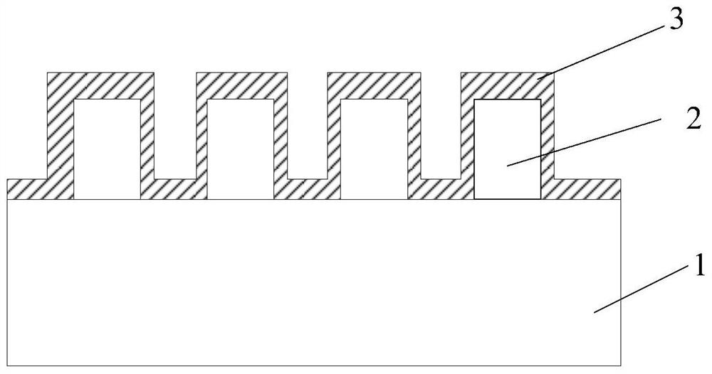
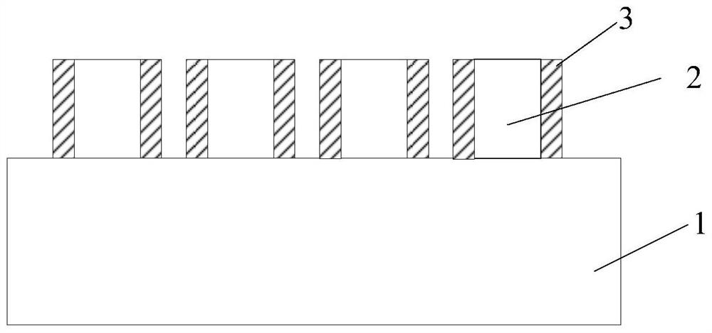
[0031] Figure 5 to Figure 11 It is a structural schematic diagram of the formation process of the semiconductor device in the first embodiment of the present invention.

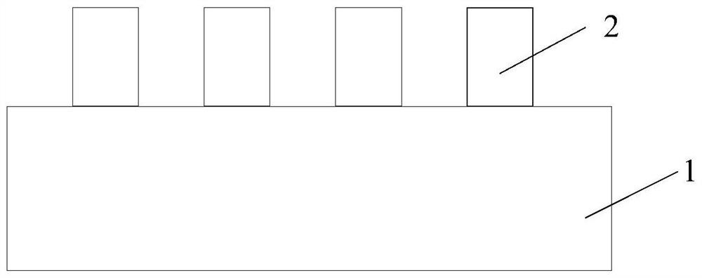
[0032] first reference Figure 5 , providing a substrate 100 on which core layers 200 are discretely arranged.

[0033] The substrate 100 may be monocrystalline silicon, polycrystalline silicon or amorphous silicon; the substrate 100 may also be semiconductor materials such as silicon, germanium, silicon germanium, gallium arsenide; in this embodiment, the substrate 100 The material is monocrystalline silicon.

[0034] In this embodiment, before forming the discretely arranged core layer 200 on the substrate 100, a protective layer 110 is formed on the substrate; in other embodiments, before forming the core layer, the The protection layer 110 is not formed on the substrate.

[0035] In this embodiment, the material of the protective layer 110 is silicon oxide; in other embodiments, the material of the p...

no. 2 example

[0074] Figure 12 to Figure 15 It is a structural schematic diagram of the formation process of the semiconductor device in the second embodiment of the present invention.

[0075] The difference between this embodiment and the first embodiment is that multiple oxidation and etching processes are used to process the sidewall layer until the substrate and the top of the core layer are exposed.

[0076] The number of times of the oxidation etching process is N times, 1≤N≤4, and N is a natural number greater than or equal to 1.

[0077] In this embodiment, N=2, that is, two oxidation etching processes are used to process the sidewall layer until the substrate and the top of the core layer are exposed; in other embodiments, three or four times can also be used. The oxidation etching process processes the sidewall layer to expose the substrate and the top of the core layer.

[0078] The process from providing the substrate to forming the side wall layer is the same as that of the f...


PUM


Abstract

The invention provides a method for forming a semiconductor device, and the method comprises the steps: providing a substrate, and forming a core layer in discrete arrangement on the substrate; forming a side wall layer on the substrate and on the side wall and the top of the core layer; processing the side wall layer by adopting an oxidation etching process until the substrate and the top of thecore layer are exposed, wherein the oxidation etching process comprises the following steps: performing oxidation processing on the side wall layer by adopting an oxidation process; and etching the side wall layer subjected to the oxidation treatment by adopting an etching process. According to the invention, the quality of the side wall layer on the side wall of the core layer is improved, and preparation is made for forming the fin part with good quality, so that the quality of the formed semiconductor device is improved.

Description

technical field [0001] The invention relates to the technical field of semiconductor manufacturing, in particular to a method for forming a semiconductor device. Background technique [0002] With the rapid development of semiconductor manufacturing technology, semiconductor devices are developing towards higher element density and higher integration. As the most basic semiconductor device, the device is being widely used at present. The control ability of the traditional planar device to the channel current is weakened, resulting in the short channel effect and causing the leakage current, which ultimately affects the electrical properties of the semiconductor device. [0003] In order to overcome the short channel effect of the device and suppress the leakage current, the prior art proposes a fin field effect transistor (Fin FET), which is a common multi-gate device, and the structure of the fin field effect transistor includes : a fin and an isolation structure located o...

Claims


Application Information

Patent Timeline
Patent Type & Authority Applications(China)
IPC IPC(8): H01L21/336H01L21/308
CPCH01L21/3086H01L29/66795
Inventor 龚申旻郑二虎张海洋
Owner SEMICON MFG INT (SHANGHAI) CORP
Why Eureka
Try Eureka