Annealing method of silicon wafer for PERC single crystal battery, silicon wafer for PERC single crystal battery and application
A technology of annealing and silicon wafers, which is applied in the field of solar cells, can solve problems such as the influence of the annealing process on the hydrophilicity of silicon wafers, and achieve good passivation effect and compact structure
- Summary
- Abstract
- Description
- Claims
- Application Information
AI Technical Summary
Problems solved by technology
Method used
Image

Examples
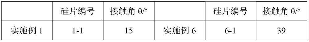
Embodiment 1
[0060] This embodiment provides a method for annealing silicon wafers for PERC monocrystalline cells and silicon wafers for PERC monocrystalline cells. The annealing method includes the following steps:
[0061] (1) Put the silicon chip into the quartz boat, push it into the furnace tube of the annealing furnace, keep the absolute pressure in the furnace tube as 1000mbar, and feed the nitrogen gas with a flow rate of 3000sccm for purging, and simultaneously feed the nitrogen gas with a flow rate of 500sccm, Make the nitrogen flow rate tend to be stable;
[0062] (2) evacuate until the absolute pressure in the furnace tube is 100mbar, and feed in nitrogen gas with a flow rate of 200sccm to purge for 190s to get rid of the waste gas around the silicon wafer in the furnace tube;
[0063] (3) Keep the absolute pressure in the furnace tube at 700mbar, and purge 290s with nitrogen gas with a flow rate of 15000 sccm to remove the residual impurities on the surface of the silicon wafe...
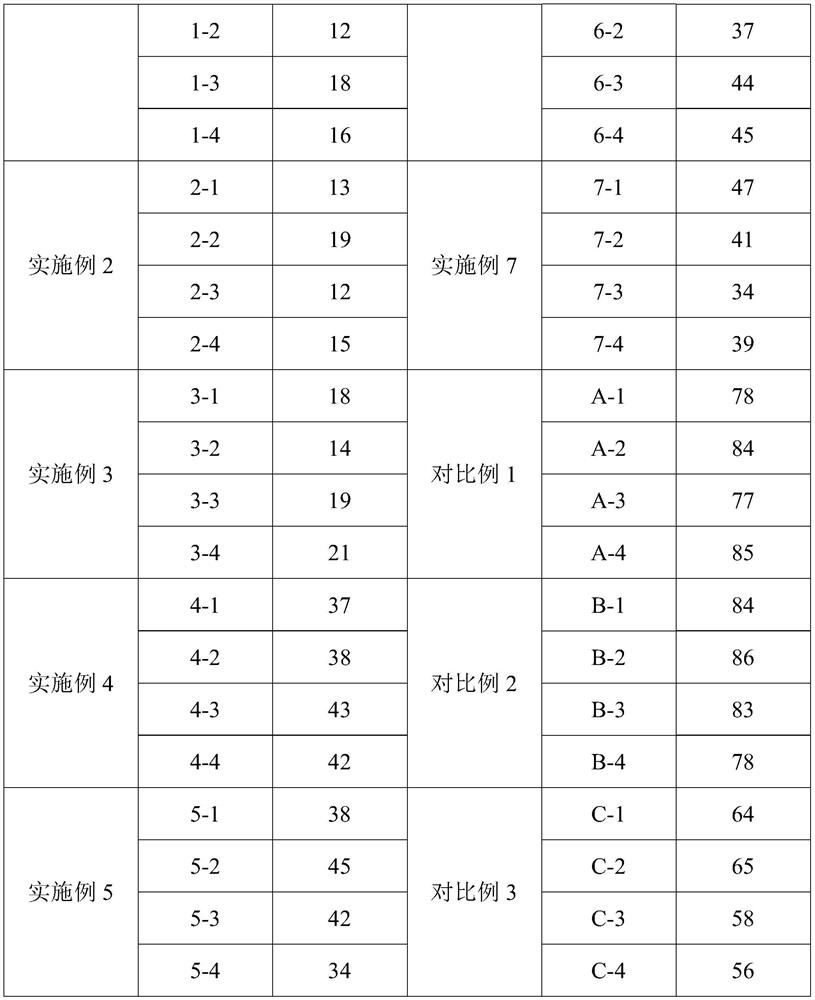
Embodiment 2
[0071] This embodiment provides a method for annealing silicon wafers for PERC monocrystalline cells and silicon wafers for PERC monocrystalline cells. The annealing method includes the following steps:
[0072] (1) silicon chip is put into quartz boat, pushes in the furnace pipe of annealing furnace, keeps the absolute pressure in the furnace pipe to be 800mbar, and feeds the nitrogen gas that flow velocity is 2500sccm to purge, and feeds the nitrogen gas that flow velocity is 450sccm additionally simultaneously, Make the nitrogen flow rate tend to be stable;
[0073] (2) evacuate until the absolute pressure in the furnace tube is 80mbar, and feed the nitrogen gas with a flow rate of 150sccm to purge for 180s to get rid of the waste gas around the silicon chip in the furnace tube;
[0074] (3) Keep the absolute pressure in the furnace tube at 650mbar, and feed nitrogen with a flow rate of 14000sccm for 280s to remove residual impurities on the surface of the silicon wafer in ...
Embodiment 3
[0082] This embodiment provides a method for annealing silicon wafers for PERC monocrystalline cells and silicon wafers for PERC monocrystalline cells. The annealing method includes the following steps:
[0083] (1) put the silicon chip into the quartz boat, push it in the furnace tube of the annealing furnace, keep the absolute pressure in the furnace tube as 1200mbar, and feed the nitrogen with a flow velocity of 3500sccm for purging, and simultaneously feed the nitrogen with a flow velocity of 550sccm, Make the nitrogen flow rate tend to be stable;
[0084] (2) evacuate until the absolute pressure in the furnace tube is 120mbar, and feed the nitrogen gas with a flow rate of 250sccm to purge for 200s to get rid of the waste gas around the silicon wafer in the furnace tube;
[0085] (3) Keep the absolute pressure in the furnace tube at 750mbar, and feed nitrogen with a flow rate of 16000sccm for 300s to remove residual impurities on the surface of the silicon wafer in the fur...
PUM
 Abstract
Description
Claims
Application Information
 - R&D
- Intellectual Property
- Life Sciences
- Materials
- Tech Scout
- Unparalleled Data Quality
- Higher Quality Content
- 60% Fewer Hallucinations
Browse by: Latest US Patents, China's latest patents, Technical Efficacy Thesaurus, Application Domain, Technology Topic, Popular Technical Reports.
© 2025 PatSnap. All rights reserved.Legal|Privacy policy|Modern Slavery Act Transparency Statement|Sitemap|About US| Contact US: help@patsnap.com