Organic light-emitting superlattice film as well as preparation method and application thereof
A light-emitting thin film and superlattice technology, which is applied in semiconductor/solid-state device manufacturing, nanotechnology for materials and surface science, nanotechnology, etc., can solve problems affecting the photoelectric properties of organic superlattice, and achieve excellent luminous intensity And the effect of stability, good contact and high film quality
- Summary
- Abstract
- Description
- Claims
- Application Information
AI Technical Summary
Problems solved by technology
Method used
Image

Examples
Embodiment 1
[0033] Preparation of Me-PTCDI / PTCDA / Me-PTCDI / PTCDA organic light-emitting superlattice thin films:
[0034] (1) Preparation of substrate: The single crystal h-BN is thinned by the traditional mechanical exfoliation method, and the thinned two-dimensional single crystal BN film is transferred to SiO with a thickness of 275nm through scotch tape. 2 a. Under the 10x objective lens through an optical microscope, a BN film with a transparent lavender color and no scotch tape residue on the surface was selected as the BN / SiO grown on the first layer of organic film 2 substrate. In this embodiment, h-BN is selected as the substrate material, because the surface of two-dimensional h-BN is flat and has no dangling bonds, and through the van der Waals interaction between two-dimensional h-BN and organic small molecules, epitaxial growth on its surface has the same flatness organic film materials.
[0035] (2) Growth of the first layer of organic luminescent film: Pour about 2.4 mg o...
Embodiment 2
[0048] The organic light-emitting superlattice film prepared in Example 1 was applied to an organic light-emitting field-effect transistor.
[0049] Using a probe, two gold electrodes with a thickness of 100nm and a length of 250μm were non-destructively transferred to the surface of the PTCDA / Me-PTCDI / PTCDA / Me-PTCDI superlattice as the source / drain electrodes of the transistor; the device was based on SiO 2 As the gate insulating layer, Si is used as the gate, and PTCDA / Me-PTCDI / PTCDA / Me-PTCDI organic light-emitting superlattice material is used as the light-emitting layer, and the following is obtained: Figure 7 An organic light-emitting field-effect transistor with the structure shown.
[0050] Because PTCDA / Me-PTCDI / PTCDA / Me-PTCDI films have extremely strong luminous intensity, they have great application prospects in the fields of display technology, optoelectronic integration, and solid-state lasers.
Embodiment 3
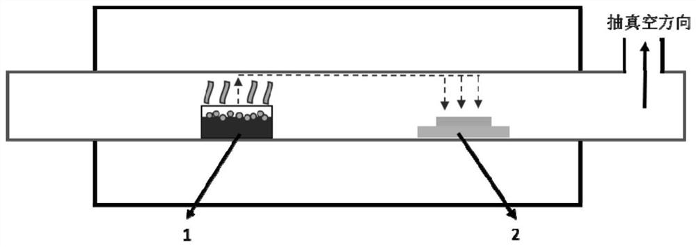
[0052] Referring to steps (1) to (2) of Example 1 to prepare Me-PTCDI organic light-emitting thin films, the difference is that in step (2), the BN / SiO 2 The substrate material was placed in the downwind area of 13cm in the air extraction direction, and the growth temperature of the Me-PTCDI thin film was set to 217°C, and the growth time was 30min. -PTCDI organic light emitting film.
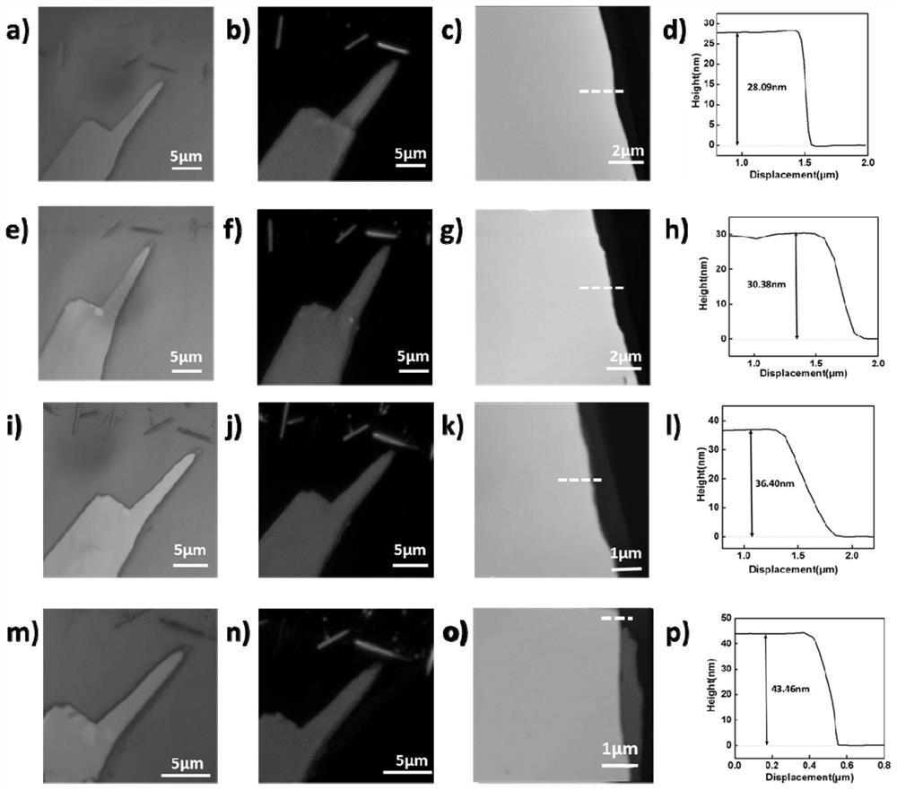
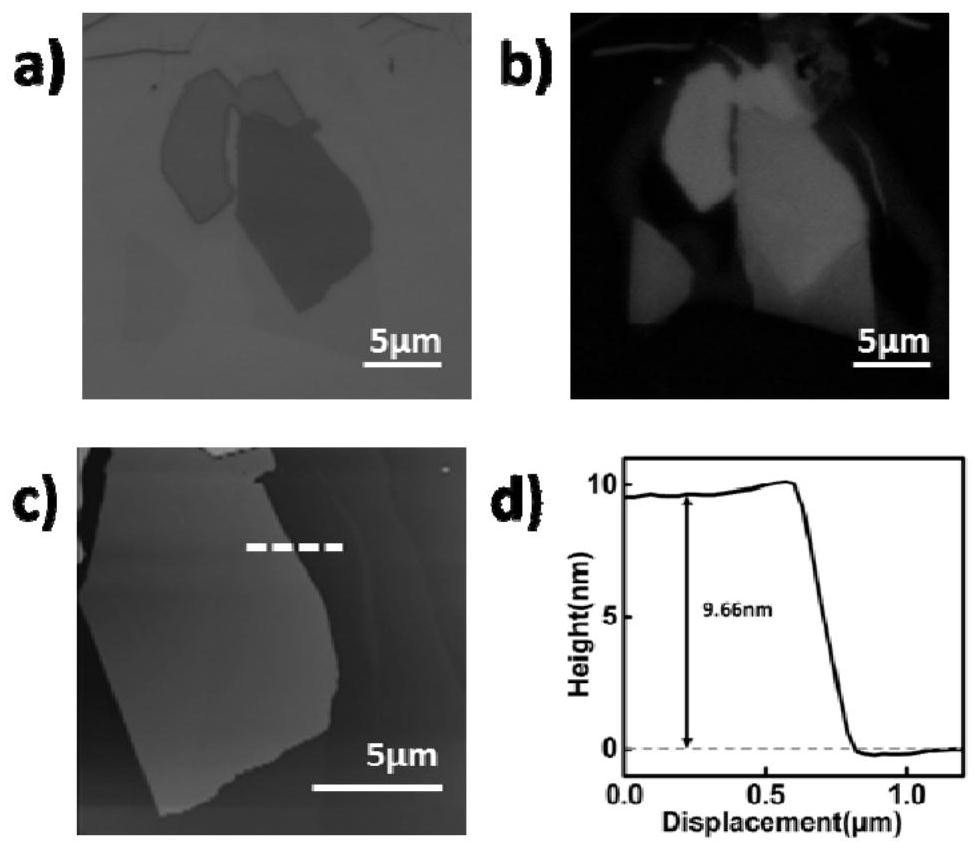
[0053] The bright field photograph under the 150 times objective lens of the optical microscope ( image 3In (a)), we found that the surface of the transparent light purple BN substrate with a thickness below 20 nm is covered with a uniform and dense dark purple region, that is, the Me-PTCDI film grown on the BN substrate. Irradiate the sample with an LED light source with a wavelength of 450nm, and the Me-PTCDI thin film area excites red fluorescence with a certain luminous brightness, such as image 3 (b). A high-quality layered Me-PTCDI luminescent film was prepared by this method.
[...
PUM
| Property | Measurement | Unit |
|---|---|---|
| Thickness | aaaaa | aaaaa |
| Length | aaaaa | aaaaa |
| Thickness | aaaaa | aaaaa |
Abstract
Description
Claims
Application Information
 - R&D
- Intellectual Property
- Life Sciences
- Materials
- Tech Scout
- Unparalleled Data Quality
- Higher Quality Content
- 60% Fewer Hallucinations
Browse by: Latest US Patents, China's latest patents, Technical Efficacy Thesaurus, Application Domain, Technology Topic, Popular Technical Reports.
© 2025 PatSnap. All rights reserved.Legal|Privacy policy|Modern Slavery Act Transparency Statement|Sitemap|About US| Contact US: help@patsnap.com