Method for growing VxC nano material by atomic layer deposition technology
An atomic layer deposition and nanomaterial technology, applied in nanotechnology, nanotechnology, metal material coating process, etc., can solve the problem of corrosion of hydrogen halide, etc., and achieve the effect of low resistivity and excellent compatibility
- Summary
- Abstract
- Description
- Claims
- Application Information
AI Technical Summary
Problems solved by technology
Method used
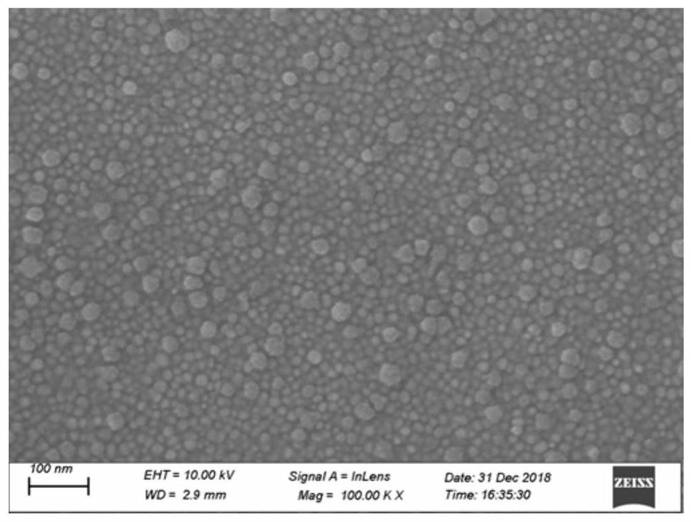
Image

Examples
Embodiment 1
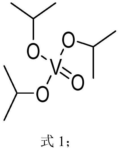
[0044] Using triisopropoxyvanadium oxide as V source and tetrahydrofuran as carbon source, V x The method for C nanomaterials comprises the following steps: taking SiO 2 As the substrate, the substrate is placed in the reaction chamber, the deposition temperature is 260°C, the triisopropoxyvanadium oxide is heated to a temperature of 70°C to vaporize it, and high-purity nitrogen is used as the carrier gas to pass into the gas phase Triisopropoxy vanadium oxide, the carrier gas flow is 10sccm, and the pulse time is 4s; After completing a pulse of step (1), use high-purity nitrogen to purge, and the purge time is 60s; carbon source tetrahydrofuran is heated to a temperature of 45°C, make it gasified, use high-purity nitrogen as the carrier gas, the carrier gas flow rate is 20sccm, pass tetrahydrofuran into the reaction chamber in pulse form, the pulse time is 1s, tetrahydrofuran reacts with the V source deposited on the substrate, get monoatomic layer V x The substrate of C na...
Embodiment 2
[0047] Using triisopropoxyvanadium oxide as the V source and diethyl ether as the carbon source, V x The method of C nanometer material, comprises the following steps:
[0048] Using silicon as the substrate, place the substrate in the reaction chamber, the deposition temperature is 280°C, heat the triisopropoxyvanadium oxide to a temperature of 75°C to vaporize it, and use high-purity nitrogen as the carrier gas to pass Into the gas phase vanadium triisopropoxide, the flow rate of the carrier gas is 20sccm, and the pulse time is 6s; after one pulse is completed, use high-purity nitrogen to purge, and the purge time is 65s; the carbon source ether is heated at 28°C to make it With high-purity nitrogen as the carrier gas, the flow rate of the carrier gas is 200 sccm, and ether is passed into in pulse form, and the pulse time is 3s; (4) after completing a pulse, high-purity nitrogen is used for purging, and the purging time is 12s, namely Complete one ALD cycle.
[0049] Repea...
Embodiment 3
[0051] Using triisopropoxyvanadium oxide as the V source and propyl ether as the carbon source, V x The method for C nanomaterials comprises the following steps: using silicon nitride as a substrate, placing the substrate in a reaction chamber, the deposition temperature is 300°C, and the heating temperature of triisopropoxyvanadium oxide is 80°C, making it gas Chemical, using high-purity nitrogen as the carrier gas, passing through the gaseous phase triisopropoxyvanadium oxide, the carrier gas flow rate is 30sccm, and the pulse time is 7s; after completing a pulse, use high-purity nitrogen to purge, and the purge time is 56s; The carbon source propyl ether is heated at 33°C to vaporize it. High-purity nitrogen is used as the carrier gas, and the carrier gas flow rate is 120 sccm. The propyl ether is passed into the pulse form, and the pulse time is 4s; after a pulse is completed, high-purity nitrogen is used. Purging is carried out, and the purging time is 36s, that is, one A...
PUM
| Property | Measurement | Unit |
|---|---|---|
| thickness | aaaaa | aaaaa |
| electrical resistivity | aaaaa | aaaaa |
| thickness | aaaaa | aaaaa |
Abstract
Description
Claims
Application Information
 - R&D
- Intellectual Property
- Life Sciences
- Materials
- Tech Scout
- Unparalleled Data Quality
- Higher Quality Content
- 60% Fewer Hallucinations
Browse by: Latest US Patents, China's latest patents, Technical Efficacy Thesaurus, Application Domain, Technology Topic, Popular Technical Reports.
© 2025 PatSnap. All rights reserved.Legal|Privacy policy|Modern Slavery Act Transparency Statement|Sitemap|About US| Contact US: help@patsnap.com