Radio frequency SiP ceramic packaging shell and manufacturing method thereof

A technology of ceramic packaging and housing, which is applied in semiconductor/solid-state device manufacturing, electrical components, electric solid-state devices, etc. It can solve the problems of increased RF signal transmission loss, increased manufacturing process steps, unfavorable RF SiP lightweight and miniaturization, etc. , to achieve the effect of improving the sealing reliability

Pending Publication Date: 2021-03-26
NO 43 INST OF CHINA ELECTRONICS TECH GRP CETC
View PDF0 Cites 4 Cited by
  • Summary
  • Abstract
  • Description
  • Claims
  • Application Information

AI Technical Summary

Problems solved by technology

However, doing so will easily cause impedance mismatch in the RF transmission line structure, resulting in increased RF signal transmission loss, and more manufacturing process steps, which will increase the weight of the package shell, which is not conducive to the lightweight and miniaturization of RF SiP.

Method used


Image

  • Radio frequency SiP ceramic packaging shell and manufacturing method thereof
  • Radio frequency SiP ceramic packaging shell and manufacturing method thereof
  • Radio frequency SiP ceramic packaging shell and manufacturing method thereof

Examples


Embodiment 1

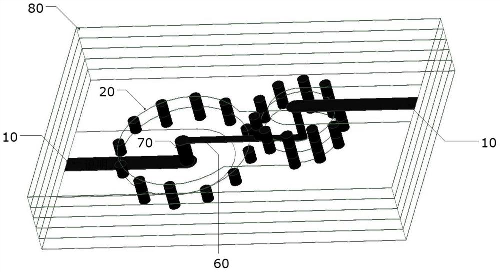
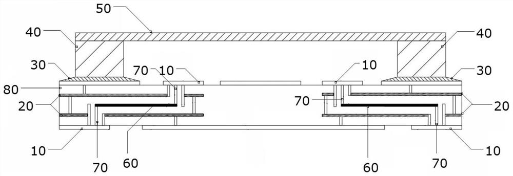
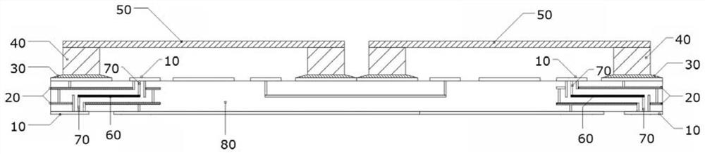
[0051] In this embodiment, the structure of the RF SiP ceramic package shell is as follows figure 2 As shown, its specific production method is as follows:

[0052] On the 8-layer LTCC green ceramic chip, according to the design pattern, each layer adopts thick film process screen printing to make interconnection vias, circuit wiring and electrical grounding patterns 20, specifically, on the third and seventh layer green ceramic chips Print the designed electrical grounding pattern 20, and the designed 4 quasi-coaxial transmission lines 70 are connected in pairs by two stripline transmission lines 60 printed on the fifth layer by screen;

[0053] Laminate 8 layers of LTCC green ceramic sheets with graphics printed on them according to the design sequence to form a substrate green body, heat and sinter at 850°C in the air for 10 minutes, then cool down to room temperature, and cut to form a package with an overall size of 9mm×9mm×0.8mm. The multilayer wiring ceramic substrate...

Embodiment 2

[0057] In this embodiment, the structure of the RF SiP ceramic package shell is as follows figure 2 As shown, its specific production method is as follows:

[0058] On the 12-layer aluminum nitride green ceramic sheet, each layer is printed and produced with interconnection holes, circuit wiring and electrical grounding patterns 20 according to the design pattern by using a thick film process. Print the designed electrical grounding pattern 20 on the 3rd layer and the 11th layer green ceramic sheet, and the designed 4 quasi-coaxial transmission lines 70 are connected in pairs by the 2 stripline transmission lines 60 printed on the 7th layer by screen;

[0059] Then, 12 layers of aluminum nitride green ceramic sheets with printed patterns were laminated according to the design sequence to form a substrate green body, which was heat-preserved and sintered at 1800°C for 4 hours in nitrogen, then cooled to room temperature, and cut into a shape of 20mm×20mm× A 1.8mm multilayer w...


PUM


Abstract

The invention discloses a radio frequency SiP ceramic packaging shell and a manufacturing method thereof, the radio frequency SiP ceramic packaging shell comprises a multi-layer wiring ceramic substrate, a metal enclosure frame and a metal cover plate, the metal enclosure frame is welded on the surface of the multi-layer wiring ceramic substrate, and the metal cover plate and the metal enclosure frame are welded and fixed so as to cover the technical enclosure frame; the multilayer wiring ceramic substrate is provided with a two-stage stepped impedance matching transmission line structure witha ground coplanar waveguide-similar coaxial-strip line-similar coaxial- strip ground coplanar waveguide, the radio frequency signal transmission insertion loss can be obviously reduced while the airtightness of the packaging shell is ensured, and the light weight and miniaturization of the packaging shell are realized.

Description

technical field [0001] The invention belongs to the technical field of integrated circuit packaging, and in particular relates to a radio frequency SiP ceramic packaging shell and a manufacturing method thereof. Background technique [0002] RF SiP (System in a Package) is a device that assembles multiple RF chips and passive devices with different functions into a standard package to realize certain system or subsystem functions. Most of the RF SiP ceramic package shells use HTCC (High Temperature Cofired Ceramic, High Temperature Cofired Ceramic) multilayer wiring substrate or LTCC (Low Temperature Cofired Ceramic, Low Temperature Cofired Ceramic) multilayer wiring substrate as the carrier of RF devices and circuits, and One or more radio frequency input / output interface circuit patterns are integrated in the ceramic substrate. [0003] The QFN RF SiP ceramic package housing is more and more used in RF SiP packages due to the integration of the RF input / output interface a...

Claims


Application Information

Patent Timeline
Patent Type & Authority Applications(China)
IPC IPC(8): H01L23/498H01L23/14H01L23/15H01L23/02H01L21/48
CPCH01L21/4817H01L23/02H01L23/14H01L23/142H01L23/15H01L23/49838
Inventor 刘俊永吴建利王伟
Owner NO 43 INST OF CHINA ELECTRONICS TECH GRP CETC
Why Eureka
Try Eureka